Over the past few years, NTT has been developing III-V/Si heterogeneously integrated EA-DFB lasers and electro-absorption modulators (EAMs), with the goal of putting them into co-packaged optics (CPO) solutions.
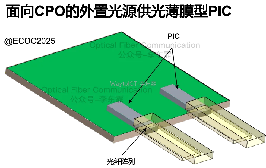
The 2025 design was explicitly aimed at CPO, achieving uncooled operation with wide-temperature and wide-wavelength tolerance. It used an external light source, which is advantageous for heat dissipation and easy replacement.
But the external light source has a cost: light must pass through the fiber interface and passive silicon photonic circuits, introducing additional coupling loss, routing loss, and mode-conversion loss. Moreover, when a single light source is shared among multiple EAMs, higher launch power is needed to compensate for splitting loss, and the problem worsens as the channel count grows.
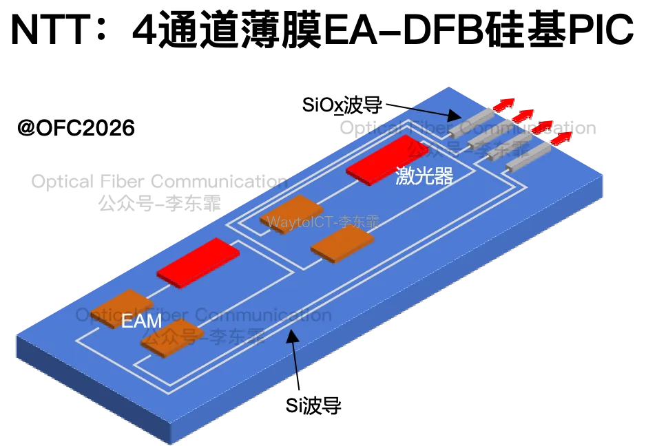
At OFC 2026, NTT integrated a membrane-structure EA-DFB light source directly into the PIC, replacing the external light source and the 1×4 splitter, and demonstrated 400 Gbit/s/lane performance.
Here is an update on NTT’s latest thin-film EA-DFB progress. At ECOC 2026, NTT continued the same idea from the first half of the year, integrating the EA-DFB inside the PIC.
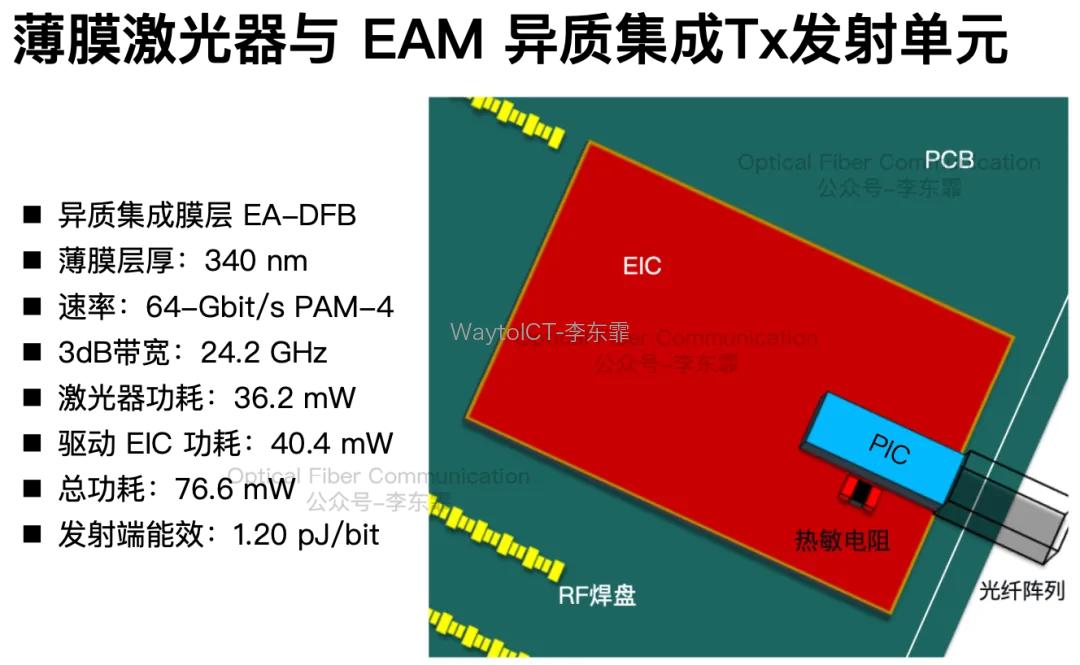
Specifically, the membrane DFB laser consumes 36.2 mW and the driver EIC 40.4 mW, for a total of 76.6 mW. At 64 Gbit/s, the Tx chiplet energy is 1.20 pJ/bit.
This PIC integrates an 8-channel EA-DFB laser array that achieves single-mode output through front and rear detuned gratings. The EAM and laser share an InGaAsP active layer; the EAM modulates the light, and a tapered transition waveguide follows for spot-size conversion to reduce coupling loss to the subsequent waveguide.
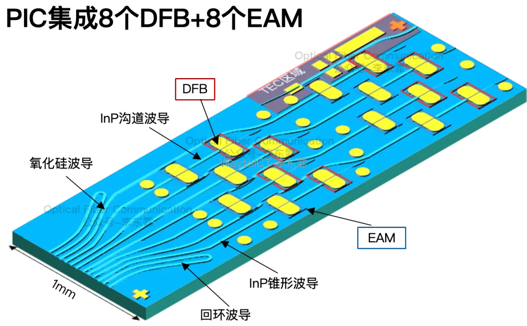
Unlike the InGaAlAs active region at OFC 2026, this one uses InGaAsP with a spectral peak around 1535 nm in the C-band.
The DFB laser is 100 um long and the EAM 100 um long, with a 250 um InP channel waveguide in between that provides electrical isolation to prevent DC bias and high-frequency RF signal crosstalk, as well as thermal isolation to keep laser heating from affecting the EAM.
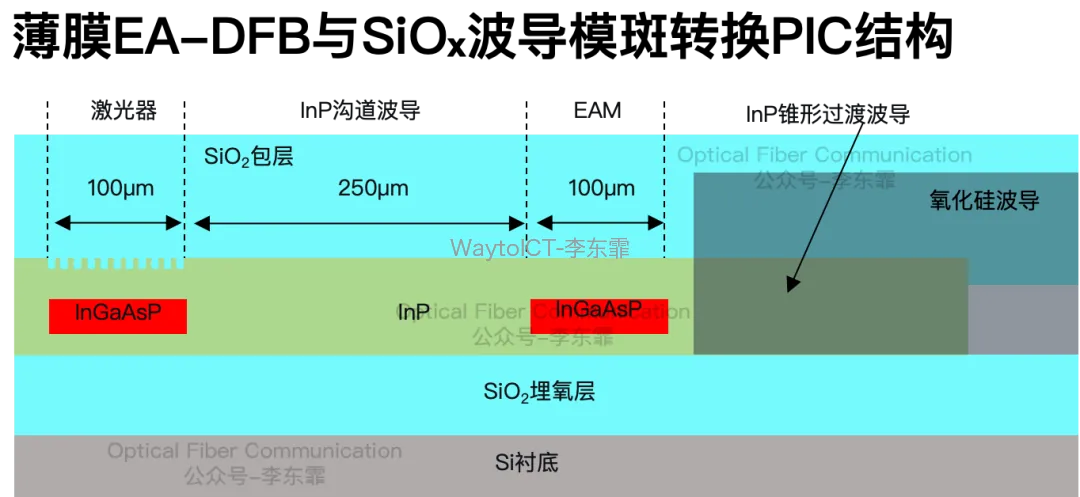
The entire InP membrane is only 340 nm thick, sandwiched by SiO2 cladding above and below, giving very strong optical confinement. For packaging, NTT embeds the EIC in the substrate, and the PIC is flip-chip bonded onto the EIC through short stacked vias.
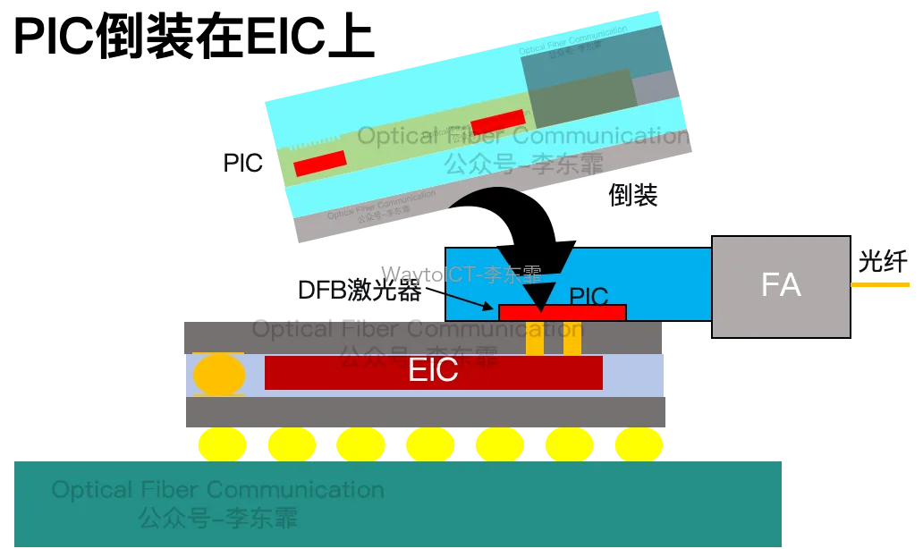
This lumped-drive design does not need a power-hungry termination resistor, making it well suited to high-density CPO integration.
When the PIC is at 35 degC, the laser threshold current is very low at only 4 mA. With the laser biased at 17 mA and the EAM biased at -0.82 V, the fiber output power is 0.29 mW.
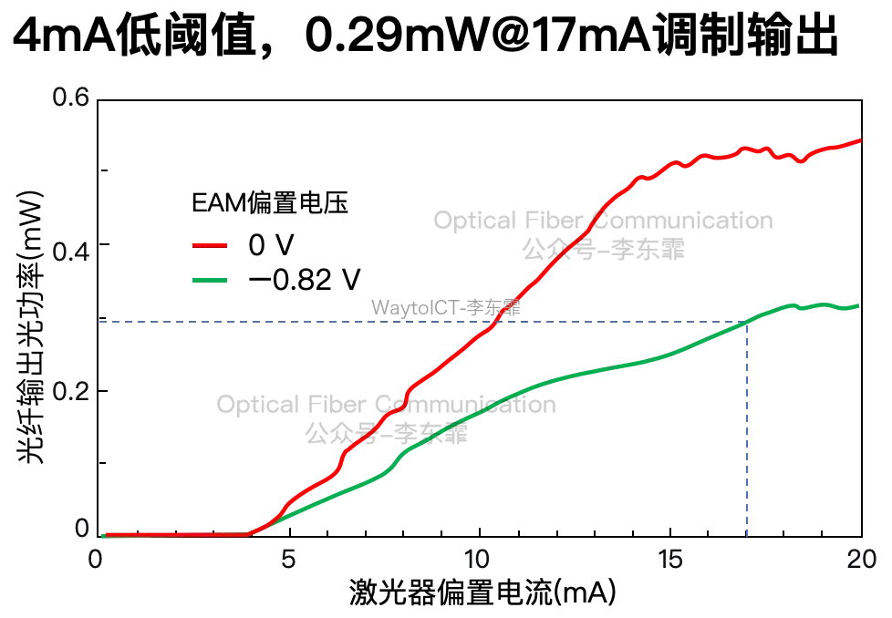
However, 0.29 mW is about -5.4 dBm, so the output power is somewhat low. For an on-PIC CPO light source in particular, power may become the bottleneck first when scaling channels or moving to higher rates.
The thin-film EAM has very low junction capacitance, with an intrinsic electro-optic bandwidth reaching 103 GHz. But NTT’s Tx transmitter module, at a 19.5 mA bias, measured a 3-dB bandwidth of only 24.2 GHz.
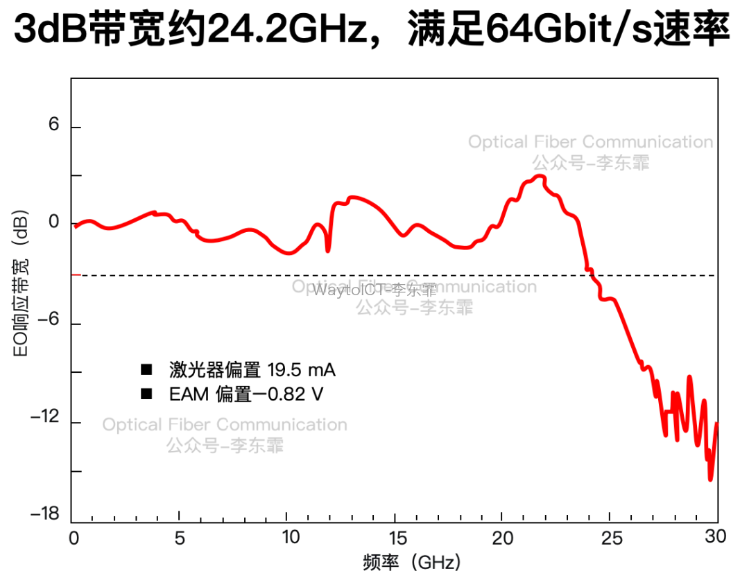
Even so, this bandwidth is fully sufficient for 32-GBaud PAM-4 (i.e., 64 Gbit/s) modulation.
Finally, NTT connected this PIC to a Ge-PD integrated Rx chiplet and verified 14 m standard single-mode fiber transmission. Fourteen meters is sufficient for CPO scale-up scenarios. On total power, the Rx-side PD-TIA is 22.3 mW, or 0.35 pJ/bit. So the system total energy is Tx (1.20) + Rx (0.35) = 1.55 pJ/bit.
Industry CPO power estimates are generally 5-6 pJ/bit, and Broadcom’s Advanced CPO roadmap reaches 5 pJ/bit only by 2029. Yole’s CPO metrics are 5-7 pJ/bit for scale-out and <1 pJ/bit for scale-up.
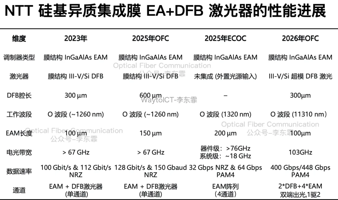
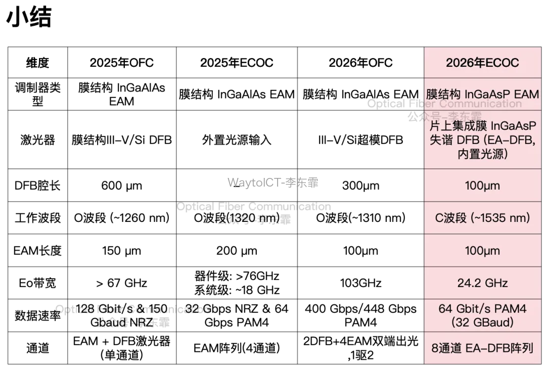
Finally, here is a summary comparison of NTT thin-film DFB + EAM modulator performance progress from 2025 to 2026.
Further Reading
- NTT: thin-film EAM electro-absorption modulator progress for CPO
- NTT: SiN-platform micro-TP tunable thin-film InP laser
References
[1] S. Yamaoka, et al., “Energy-Efficient Optical Chiplet Link with Heterogeneously Integrated Membrane EA-DFB Laser Achieving 1.55 pJ/bit at 64-Gbit/s PAM-4,” ECOC 2026.
[2] T. Hiraki, et al., “Optical Chiplet with 0.75-pJ/bit Transmitter Using Membrane III-V Electro-absorption Modulators on Si and Differential CMOS Driver,” ECOC 2025.
[3] T. Aihara, et al., “4-ch x 400-Gbps PAM4 O-Band Membrane InGaAlAs EA-DFB Laser Array on a Si Photonics Platform,” OFC 2026, paper Th4A.1.
[4] T. Minotani, et al., “Over-8000-GHz-ohm/mW-FoM Transimpedance Amplifier for Processor Interconnection,” OFC 2026, paper Th2A.2.
[5] Broadcom, OFC 2025.
[6] Yole, Co-packaged Optics for Data Centers, 2025.
Enjoy this article?
Subscribe to get new optical communication insights delivered to your inbox. Free, unsubscribe anytime.