If you are interested in semiconductors / chips / optical components & modules / optical fiber communications
Welcome to follow us!
In a modulator, the basic idea behind changing light intensity is to rely on the interference of two light beams – when the interference is constructive, it is “1”, and when destructive, it is “0”.
To produce interference, we essentially need a phase difference between the two light beams.

Where does the phase difference come from? It comes from the optical path difference, which is essentially the product of “refractive index x length”.
Therefore, to change the optical path difference, we either change the refractive index of the material or directly change the physical length the light travels.
Taking the Mach-Zehnder modulator as an example, the following type achieves modulation by directly changing the physical length ΔL.
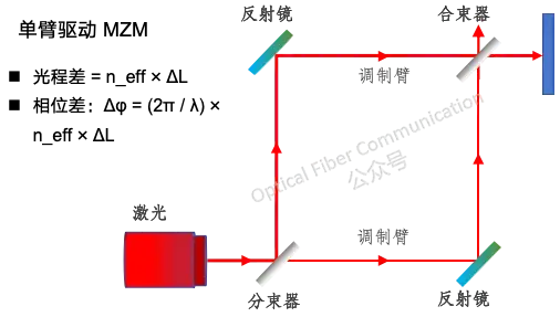
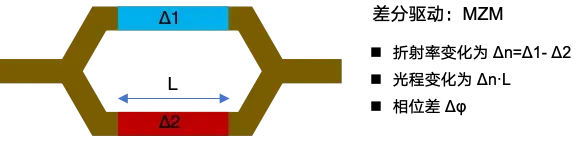
Another common approach is to use an electrical signal to control the refractive index change Δn of the material. Here we can tune only one arm, or tune both arms together in opposite directions – this is differential driving, also called push-pull modulation, which is more efficient.
Reference:
HG Genuine: Differential Package Optical Module Solution
ZTE: Mach-Zehnder Modulators and CPO White-Box Switches
Seen this way, electro-optic modulators that rely on changing the refractive index (Δn) can indeed be made more compact in theory than devices that purely rely on changing the length (ΔL).
But here is the problem: whether it is the plasma dispersion effect in silicon or the electro-optic effect in lithium niobate, the refractive index change Δn per unit length they can induce is extremely small.
To reach the “on” and “off” states, we need to accumulate a phase difference of π. According to the formula, when Δn is very small, the length L of the modulation region must be large enough to accumulate this phase difference.
Similarly, in a microring modulator, we can also shift the resonance condition by changing the effective refractive index neff of the waveguide or the ring radius R, thereby achieving intensity modulation.
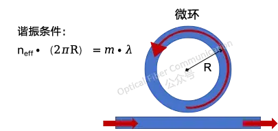
Reference: Microring Resonators: Coupling, Modulation and Wavelength Division Multiplexing
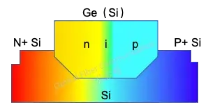
But when the application scenario has extremely stringent size requirements, such as at the transmit end of an optical module, the above devices that rely on slowly accumulating phase through refractive index are hard to shrink further. At this point, the electro-absorption modulator based on germanium-silicon material becomes a very attractive solution.
So why can the electro-absorption modulator be made smaller? Fundamentally, it modulates the light intensity directly, unlike the MZM which needs to first adjust the phase and then convert it through an interference structure. It has no additional interference arm, and its structure is simple.
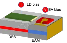
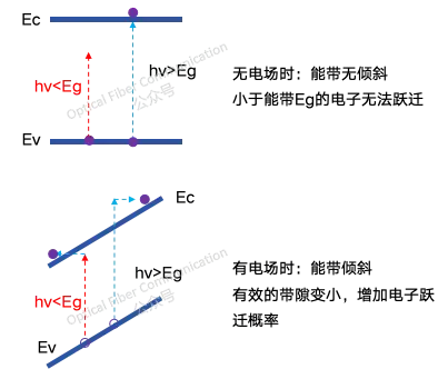
Taking the EML modulator as an example (EML = DFB + EAM), its modulation section fundamentally uses the Franz-Keldysh effect: when an electric field is applied, the energy band of the material tilts, which is equivalent to a reduction in the effective band gap.
As a result, photons that originally had energy slightly below the band gap and should have passed through now have a greatly increased probability of being absorbed, manifested as a drastic change in the absorption coefficient α.
For an ideal optical switch, we of course hope that in the “on” state the light almost completely passes through (absorption coefficient α very low), and in the “off” state the light is efficiently absorbed (absorption coefficient α very high).
To make the most commonly used C-band (around 1550 nm) work efficiently, the material needs to be “tailored”.
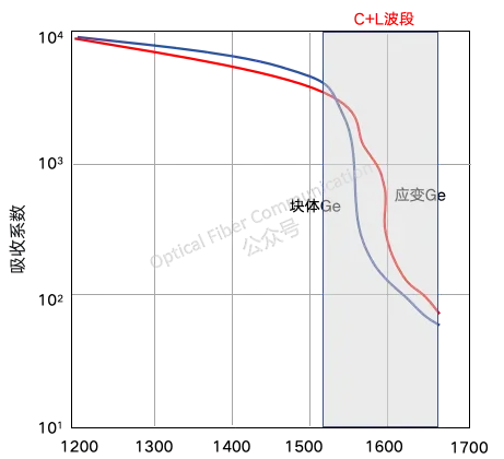
A major method is to dope in a certain proportion of silicon to form a germanium-silicon alloy. The introduction of silicon increases the band gap of the material, thereby shifting the entire absorption edge toward shorter wavelengths and tuning it to the C-band.

In actual operation, we change the absorption coefficient by changing the bias voltage.
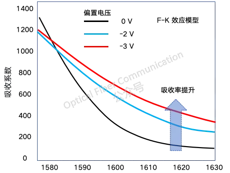
Corresponding to the device state, at 0V the absorption may be low (light passes through, “on”), and at -2V the absorption is high (light is blocked, “off”).
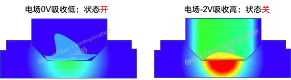
It is precisely because of this direct absorption modulation mechanism that the germanium-silicon electro-absorption modulator does not require a long interaction distance, and its size can be made very small – the core region needs to be only tens of microns long, making it ideal for high-density integration.
However, we should distinguish the different requirements of modulators and photodetectors here; the detector’s requirements are exactly the opposite.
For the detector, we want the absorption in the target band to be as high and as flat as possible. The response of a pure germanium detector drops off on the long-wavelength side, so the industry uses techniques such as introducing a strain layer to make wideband high-speed detectors that cover both the C and L bands.
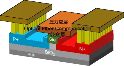
For how to achieve this, see Huawei: C+L-Band 100G Bandwidth Germanium-Silicon Photodetector with Strain Layer
Thanks for reading!
Add WeChat WaytoICT to join the Semiconductor & Optical Component Industry Chain Group 2.
Welcome to join our community and access a wealth of high-value technical documents and trend research reports in the fields of semiconductor chips, optical components, and optical modules!

Related Reading
- NTT: Progress on Thin-Film EAM Electro-absorption Modulators for CPO
- What Is an EML? Working Principle, Applications, and Evolution of Electro-absorption Modulated Lasers
- It Turns Out to Be So Simple: Mach-Zehnder M-Z Modulators
Enjoy this article?
Subscribe to get new optical communication insights delivered to your inbox. Free, unsubscribe anytime.