
If you are interested in semiconductors / chips / optical components & modules / optical fiber communications
Welcome to follow us!
Below we share Broadcom’s progress in developing 200 Gbps PAM4 850nm VCSELs.
Further reading:
Tencent’s 3.2T NPO Technology Evolution and Scale Out/Up Roadmap
Huawei HiSilicon: Silicon Photonics and VCSEL Evolution Roadmap, CPO and NPO Progress
Broadcom & HiSilicon: VCSEL NPO/CPO and Silicon Photonics CPO
As AI-scale networks expand, the scale of connectivity continues to grow, requiring optical interconnect technology to support longer distances. Energy efficiency, reliability, bandwidth density, and cost are important considerations driving the widespread adoption of optical interconnect. To support AI-scale networks, Broadcom has proposed a near-package optics (NPO) solution based on VCSELs.
In terms of device design and manufacturing, to understand the bandwidth and noise requirements of multi-mode links, Broadcom built a model to simulate VCSELs operating in 200 Gbps links. Simulation results show that when the VCSEL’s -3dB bandwidth exceeds 35 GHz and the relative intensity noise is below -152 dB/Hz, a clear eye diagram can be expected at 106.25 GBd.
Based on the bandwidth and noise targets set by simulation for the 200 Gbps VCSEL, Broadcom designed a VCSEL capable of supporting 200 Gbps modulation. It inherits the design foundation of the previous-generation 100 Gbps PAM4 VCSEL, while improving bandwidth, reducing noise, and optimizing thermal resistance to reduce junction temperature rise. The VCSEL uses an oxide layer for carrier and photon confinement, formed by wet lateral oxidation of a high-aluminum-content layer after trench etching. Broadcom also adopted a multi-energy ion implantation process to reduce pad capacitance, with a structure similar to previously published designs.
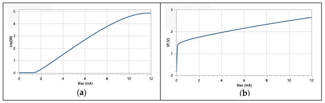
Next, let’s look at the specific results. Broadcom characterized the fabricated 200 Gbps devices. A typical VCSEL at 9 mA produces an optical power exceeding 3 mW with a voltage of about 2.5 V.
The VCSEL’s design optimizes dynamic performance from four aspects:
- Improving the differential gain, which determines the maximum resonant frequency and bandwidth;
- Improving carrier transport in the p-n diode;
- Optimizing the cavity detuning between the Fabry-Perot cavity resonant wavelength and the material gain peak, which determines the behavior of threshold current versus temperature;
- Improving thermal resistance to lower the junction temperature under operating bias.
Broadcom measured the small-signal modulation response of the 200 Gbps VCSEL by probing directly on the wafer. The results show that at 9 mA its -3 dB bandwidth exceeds 35 GHz, with a flat, well-damped response. One of the challenges in increasing the bandwidth of directly modulated lasers comes from the impact of electrical parasitics such as capacitance and resistance. By reducing these parasitics, the optical modulation bandwidth of the VCSEL has the potential to exceed 45 GHz.
Since VCSEL noise is the main source of total link noise, Broadcom improved the design to minimize power fluctuations caused by inter-mode competition and other effects, thereby reducing VCSEL noise. The design optimization reduced the relative intensity noise of the 200 Gbps PAM4 VCSEL to below -152 dB/Hz.

In terms of large-signal performance, Broadcom used an arbitrary waveform generator to generate a 106.25 GBd PAM4 signal and measured it with a multi-mode optical oscilloscope. Eye diagram tests show that clear, open eye diagrams are obtained when using fibers with different effective mode bandwidths, including 2-meter OM4, 30-meter standard OM4, and 50-meter custom high-bandwidth fiber.
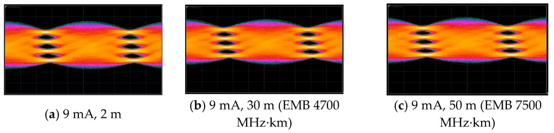
This shows that the combined bandwidth of the VCSEL and fiber is sufficient to support 200 Gbps operation. Using custom fiber with a bandwidth of 7500 MHz-km helps extend the transmission distance of the 200G link to 50 meters. Currently, the multi-mode 200 Gbps link distance standard has not yet been formally determined by IEEE.
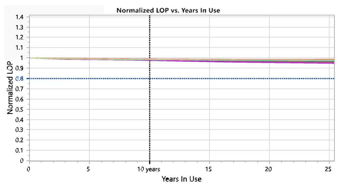
In terms of reliability, a key factor in achieving excellent wear-out lifetime is lowering the junction temperature. Broadcom addressed this challenge by using lower-thermal-resistance materials in the DBR design. Preliminary reliability tests on the 200 Gbps PAM4 VCSEL show that under operating conditions of 60 degrees Celsius and 9 mA, its output power shows a gradual decline over time, similar to what was observed for the 100 Gbps VCSEL. More comprehensive reliability testing is ongoing to confirm the acceleration model and provide more adequate lifetime statistics.
Further reading: Broadcom: 51.2T CPO Reliability Data and 102.4T CPO Switch
At the application level, VCSEL-based optical interconnect has widely supported short-distance front-end networks since the 1 Gbps era. As AI cluster scale continues to grow to meet increasing computing demands, the copper interconnect commonly used in scale-out networks today will be limited to within a single rack due to high electrical insertion loss. Optical interconnect technology, by converting electrical signals to optical signals for transmission in fiber, can achieve longer distances across racks.
In AI-scale networks, to support massive memory transfer between accelerators for efficient parallel computing, enormous interconnect bandwidth is required. For example, the Blackwell GPU generation may require up to 28.8 Tbps of bandwidth. Direct-attach copper supporting 100 Gbps per SerDes channel is limited by signal impairments such as jitter and insertion loss, with a transmission distance of only 4 to 5 meters. The next-generation 200 Gbps per-channel SerDes, due to higher Nyquist frequency loss, will further limit the effective distance of copper to about 1 to 2 meters. Although retimers can extend the distance to 7 meters, this increases cost and power consumption.
Therefore, copper interconnect limits XPU connections to within one rack, or at most across two racks, thus limiting the number of XPUs that can be connected within a single hop. In contrast, optical interconnect can support distances of 50 meters and beyond at high per-channel rates, making it possible to simplify the architecture through network disaggregation.

To adopt optical interconnect in scale-out networks, several key parameters need to be considered: energy efficiency, reliability, bandwidth density, and cost. The passive copper interconnect currently used in scale-out networks has no active power consumption, while optical interconnect contains active laser devices and requires electro-optic conversion. To achieve a reasonable balance between power consumption and distance, the energy efficiency of optical interconnect should be as high as possible. Reliability is critical for maximizing XPU utilization; unlike scale-out networks that can retransmit frequently, scale-up networks require stable and reliable interconnects to minimize the frequency of checkpoint recovery.
As XPU bandwidth increases to 50 Tbps and above, high-density interconnect needs to be achieved within limited front-panel width, with a desired bandwidth density greater than 0.6 Tbps/mm. Finally, the cost of optical interconnect should be reasonable and comparable to copper interconnect.
To this end, Broadcom proposes a VCSEL-based NPO near-package optical engine concept solution with a total bandwidth of up to 3.2 Tbps.

See also: Broadcom & HiSilicon: VCSEL NPO/CPO and Silicon Photonics CPO
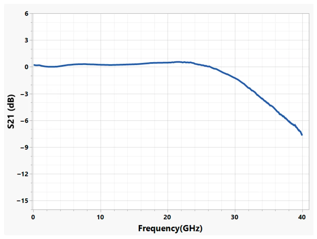
Inside this independent package are integrated four 1×8 VCSEL arrays with drivers, four 1×8 photodetector arrays with amplifiers, and a microcontroller unit. Each channel supports 100 to 128 Gbps data rate, requiring a Nyquist frequency above 32 GHz. The figure below shows that the 100G VCSEL can still meet this requirement at a high temperature of 75 degrees Celsius.
The transmit and receive parts can be packaged separately as independent engines. The VCSEL and detector arrays are connected to the engine substrate through wire bonding, and the light is vertically coupled into multi-mode fiber through low-cost plastic array lenses. Using CMOS-based drivers and amplifiers achieves high energy efficiency, with the total energy efficiency including the VCSEL at about 1 pJ/bit, meaning each NPO device consumes less than 4W, far better than silicon photonics solutions with energy efficiency of 5-10 pJ/bit. One reason for the higher power consumption of silicon photonics solutions is that single-mode DFB lasers require higher drive current to inject sufficient optical power for the silicon modulator.
Currently, more than 100 million 50G/100G VCSEL channels have been shipped, with cumulative field service time exceeding five trillion hours, and no returns related to VCSEL reliability, with a failure rate below 0.1 FIT, meaning the reliability risk to the overall NPO device is extremely low. Although evaluating the overall failure rate at the NPO device level still requires further analysis, it is expected that with CMOS processes and mature multi-mode manufacturing capabilities, the failure rate will be comparable to active copper interconnect.
The figure below shows an example of deploying 18 VCSEL NPO engines, supporting up to 73.7 Tbps of XPU bandwidth through a single-side interface.
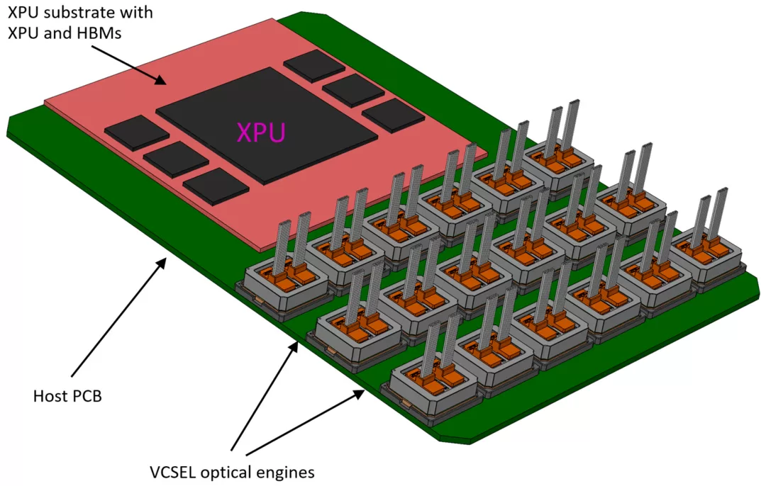
These engines are arranged in a 3×6 configuration, with each row about 120mm wide, achieving a bandwidth density greater than 0.6 Tbps/mm. The fibers can be routed to the server front panel or backplane, and can be flexibly provisioned in fiber switch boxes inside the server or at the top of the rack to accommodate the optical connection needs of different applications.
In PAM4-based optical interconnect, the digital signal processing chip is one of the main cost sources. Since NPO links are short and have low electrical insertion loss, no DSP is needed to correct signal impairments. Compared with standard optical modules at the same rate, NPO’s smaller size helps further reduce material costs. In addition, the optical lens design for one-dimensional arrays is simpler than multi-dimensional arrays, which helps control manufacturing costs. In large-scale production, its cost per Gbps is expected to be comparable to active copper cables.
In terms of design considerations, NPO links differ from standard optical links in that their electrical insertion loss budget depends on the SerDes capability of the XPU. But the advantage of NPO is its proximity to the SerDes, which limits the maximum insertion loss.
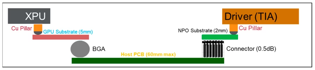
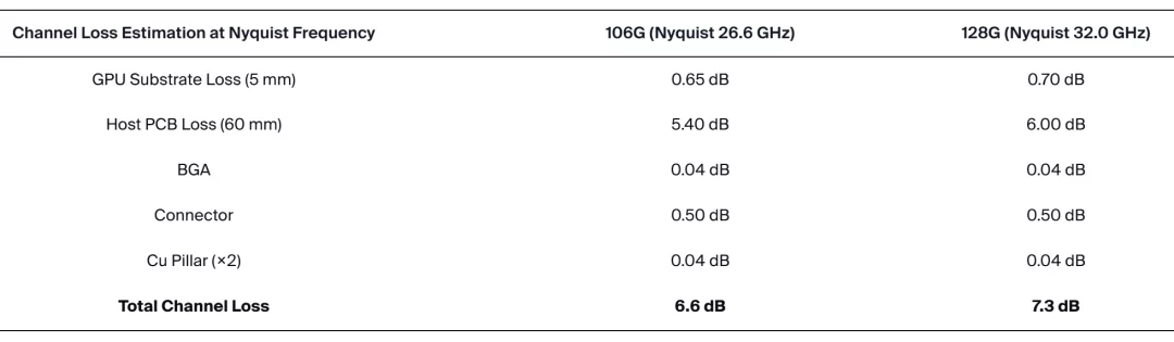
For example, when deploying 18 engines, the longest electrical trace from the SerDes is about 65 mm, which can achieve an insertion loss of about 7dB at 106 Gbps using low-loss materials; the nearest engine trace is only about 15mm, with an insertion loss of about 2dB. Compared with the 8-16dB loss range specified by the IEEE standard, the lower loss of the NPO solution and the smaller loss variation between the XPU and NPO reduce the requirements on SerDes performance.
In summary, Broadcom’s characterization of the fabricated 200 Gbps PAM4 VCSEL demonstrates excellent performance, validating the key design optimizations implemented to meet high-speed data transmission needs. Its successful high-speed performance is directly attributable to several design improvements, including enhanced differential gain, optimized carrier transport, precise cavity detuning control, and reduced thermal resistance. The small-signal modulation response confirms the device’s high-speed capability, with a -3 dB bandwidth exceeding 35 GHz and a flat, well-damped response characteristic.
At the same time, by reducing VCSEL noise and controlling relative intensity noise below -152 dB/Hz, it is critical for reducing the total link noise. In large-signal operation, the VCSEL demonstrates clear eye diagrams across various fiber types and lengths, with transmission distances extendable to 50 meters.
Preliminary reliability tests show a gradual degradation trend similar to the previous-generation 100 Gbps VCSEL, indicating a robust design.
Furthermore, the NPO’s layout close to the SerDes limits the maximum electrical insertion loss to a narrow range of 2-7dB; compared with the 8-16dB loss of standard optical modules, this advantage significantly reduces the requirements on SerDes performance and simplifies the overall system design.
This article is based on a paper Broadcom presented at the 29th VCSEL Conference.
Other NPO/CPO related reading:
Furukawa: Progress on ELSFP External Light Source Solutions Supporting CPO
NTT: Progress on Thin-Film EAM Electro-absorption Modulators for CPO
Quantum Wells and Quantum Dots, Innolume’s High-Power CPO Quantum Dot Lasers
HiSilicon / Intel: SiN-SOI Microring Modulators for CPO
Cisco: Pluggable CPO Optical Interface Solution
OCP2025/ECOC2025 Views on “Modulators and LPO/CPO”
Glass Substrates: Pluggable Connection Solutions in CPO Packaging
e-Tube Plastic Waveguide Solution Supporting CPO
Nubis: 1.6T CPO Optical Engine Technology Based on 2D Fiber Arrays
Accelink: Some Views on CPO and Its 3.2T Silicon Photonics CPO Solution
Samtec: CPX Supporting CPC + CPO
Marvell’s Views on Scale Up/Out + 102.4T CPO Switch
Nvidia: CPO External Light Source Coupling Scheme with Polarization Tracker
UESTC: CPO Co-Packaging Solution Based on Micro-Channel Liquid Cooling
Google/Coherent and Others: Pluggable vs. CPO vs. OCS
CAICT Views on Silicon Photonics CPO and the Evolution of 400G per-Channel Technology
ZTE: Reliable Installation and Heat Dissipation Solution for CPO External Light Sources
ZTE: Mach-Zehnder Modulators and CPO White-Box Switches
CPO Package Structure Based on Glass Carrier Boards
A CPO Optical Engine Package Structure with Pluggable Fiber
If you are interested in semiconductors / optical components / optical modules / optical fiber communications
Welcome to follow us!
Enjoy this article?
Subscribe to get new optical communication insights delivered to your inbox. Free, unsubscribe anytime.