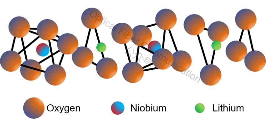
There are quite a few methods for preparing thin-film lithium niobate (TFLN), such as CVD, MBE, PLD, and sputtering. However, these tend to either produce grain boundaries and defects or have inaccurate lithium-niobium ratios.
So for making devices like optical modulators and waveguides, we generally use the Smart Cut process.
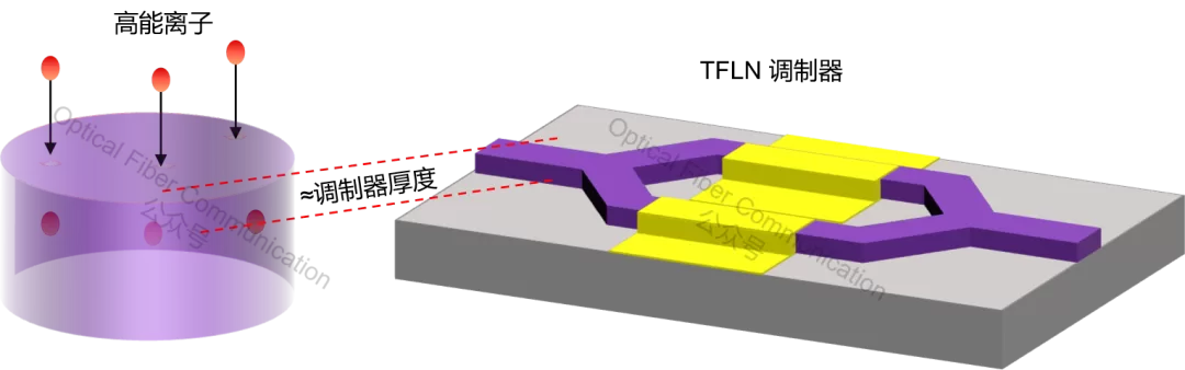
The basic principle of this process is very simple. The first step is to bombard high-energy helium or hydrogen ions into the lithium niobate crystal at high speed.
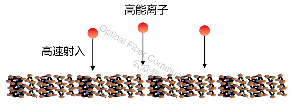
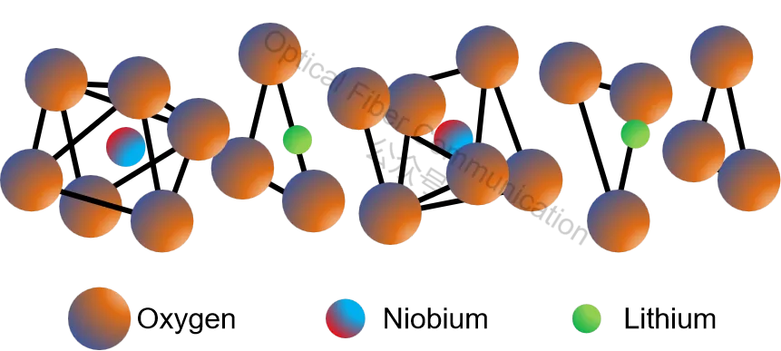
Note that the atoms in the lithium niobate crystal are only a fraction of a nanometer apart, so there is no large gap for ions to pass through smoothly.
Thin-Film Lithium Niobate Basics & Huawei HiSilicon’s 540Gbps SiN-SOI-TFLN
So for the ions to enter, they can only forcefully knock away the surrounding atoms to carve out a path – the so-called “might makes a miracle”.
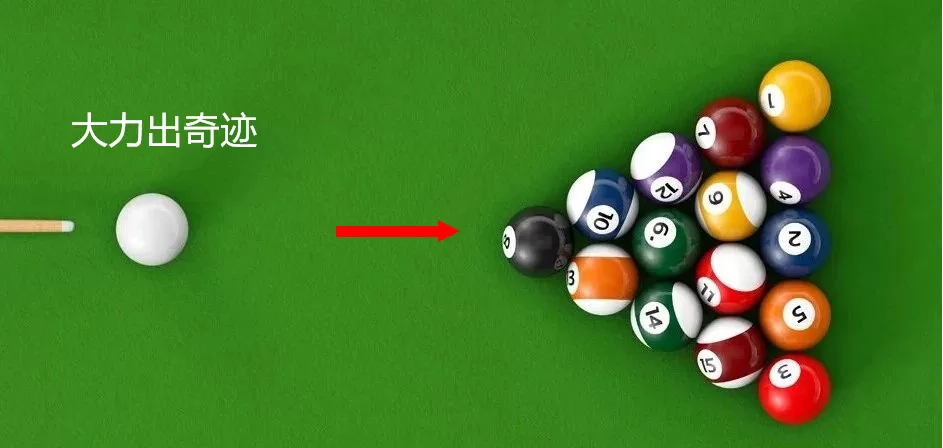
After the ions collide in at high speed, their energy is lost gradually, not all at once. They eventually stop at a certain depth inside the lithium niobate crystal, and this depth is roughly the thickness of the TFLN modulator we want to make.
HyperLight/Ciena: TFLN Process Progress and Coherent Lite 12.8T XPO Solution
Nokia: TFLN Two-Electrode Modulator Solution Supporting Single-Ended/Differential Driving
Whatever thickness of film you want, you inject the ions to that depth, then do a CMP polish to grind off a few tens of nanometers from the surface to make it smooth.
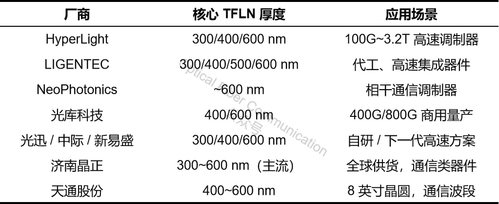
Below are the commonly used thicknesses of TFLN modulators from various manufacturers (for reference).
Hisense: 400Gbps TFLN Thin-Film Lithium Niobate Modulator Supporting 3.2T Optical Modules
Let’s talk more about the ion implantation process. After the ions are shot in from the surface, their speed slows as they travel deeper. At this point, the energy transfer efficiency of each collision becomes much higher, able to directly knock lattice atoms out of their original positions, leaving behind many vacancies and interstitial atoms.
This is similar to a bullet hitting a wooden board: the surface may only have a small hole, but deep inside it may be shattered.
Once the ions stop, a defect layer containing hydrogen or helium ions forms inside the lithium niobate wafer. Next, the implanted lithium niobate wafer is directly bonded to a silicon / SiO₂ target substrate.
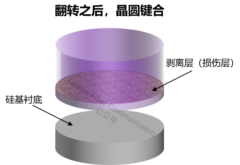
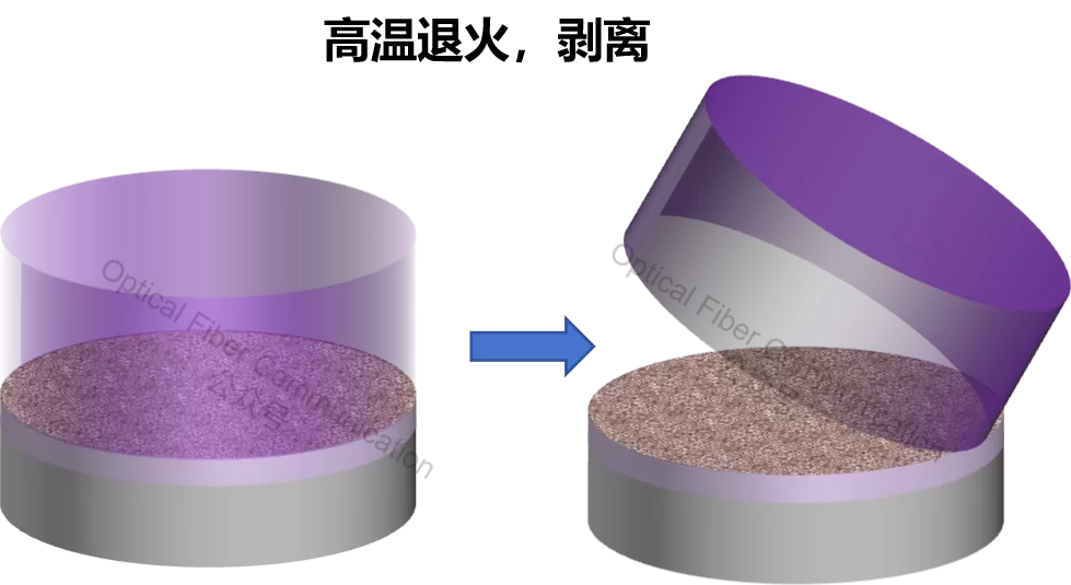
After bonding, high-temperature annealing at 200-400°C is performed to make the hydrogen or helium bubbles inside expand, so the lithium niobate thin film can be peeled off along the defect layer.
As mentioned earlier, ion implantation not only damages the crystal surface, but the internal damage is more severe. So the lattice damage must be repaired afterward, which requires a second annealing.
The first annealing mainly makes the film split apart; the second annealing uses a higher temperature so that the atoms have enough kinetic energy to return to their lattice positions and reset the interstitial atoms, thereby restoring the original electro-optic performance of the lithium niobate.
Thanks for reading!
Add WeChat WaytoICT to join the Semiconductor & Optical Component Industry Chain Group 2.
Welcome to join our community and access high-value technical documents, trend research reports, and various supply-demand business opportunities in the fields of semiconductor chips, optical components, and optical modules.

If you are interested in semiconductors / optical components / optical modules / optical fiber communications
Welcome to follow us!
Related Reading
- Hisense: 400Gbps TFLN Thin-Film Lithium Niobate Modulator Supporting 3.2T Optical Modules
- Thin-Film Lithium Niobate Basics & Huawei HiSilicon’s 540Gbps SiN-SOI-TFLN
- Nokia: TFLN Two-Electrode Modulator Solution Supporting Single-Ended/Differential Driving
Enjoy this article?
Subscribe to get new optical communication insights delivered to your inbox. Free, unsubscribe anytime.