In previous articles, we introduced the basic structure of optical modules, including TOSA, ROSA, and BOSA. Today we continue to introduce the photodetector in the ROSA optical component.
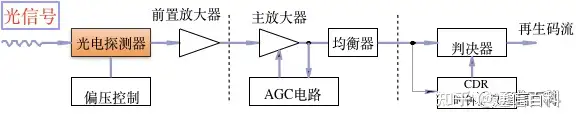
For the receiving end of an optical module to correctly identify signals and complete optical-to-electrical conversion, it needs a photodetector. The photodetector completes the optical/electrical signal conversion by detecting the optical power shining on it. The PIN photodiode and APD (avalanche) photodiode we commonly use are photodetectors. To talk about detectors, we must talk about the basic structure of the detector: the PN junction.
PN Junction
A PN junction refers to the space charge region formed at the junction of P-type and N-type semiconductors fabricated on the same semiconductor substrate. Let’s first look at what P-type and N-type semiconductors are.
P-type semiconductor: contains a relatively high concentration of “holes” (holes are equivalent to positive charges), so the P stands for Positive, making it a conductive substance;
N-type semiconductor: contains a relatively high concentration of electrons, and its conductivity is provided by free electrons. Since electrons are negatively charged, it is Negative, the N.
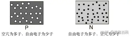
Therefore, at the junction of the P-type and N-type semiconductors, a concentration difference of electrons and holes appears, forming the diffusion movement of holes and electrons, causing some electrons to diffuse from the N-type region to the P-type region, and some holes to diffuse from the P-type region to the N-type region. The final result is a space charge region electric field formed at the PN junction (internal electric field, pointing from N to P), also called the PN junction (lacking “majority carriers,” also called the depletion layer).
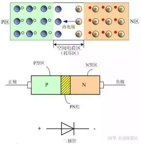
(Image from the internet)
Let me explain the internal electric field here. The formation of this electric field leads to the drift movement of carriers: first, holes in the N region drift toward the P region, and second, electrons in the P region drift toward the N region.
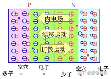
(Image from the internet)
Therefore, the diffusion movement of a simple PN diode only occurs near the PN junction, and there is no electric field far away from the PN junction. This is also why the photoelectric conversion efficiency of PN diodes is low and the response speed is slow.
PIN Photodiode
To solve this problem and improve conversion efficiency and response rate, a lightly doped N-type material I (Intrinsic) layer is added between the P-type and N-type semiconductors to widen the depletion layer and improve conversion efficiency. This is because the lightly doped I layer has a very low electron concentration, and after diffusion it can form a very wide depletion layer. This is our PIN photodiode.
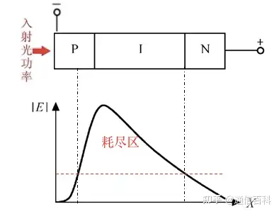
PIN photodiode
Principle:
(1) Photons illuminate the semiconductor material to generate photo-generated carriers;
(2) The photocurrent forms an electrical signal under the action of the external circuit and is output.
APD Avalanche Photodiode
In previous articles, we said that the APD avalanche photodiode has high receiver sensitivity, and this high sensitivity relies on the avalanche multiplication effect on the primary photocurrent. Speaking of avalanche, the first impression in everyone’s mind is probably an avalanche on a snowy mountain. It is actually the same principle: a bit of snow on a high mountain collides and accumulates from top to bottom, with the snowball getting bigger and bigger, finally forming an avalanche.
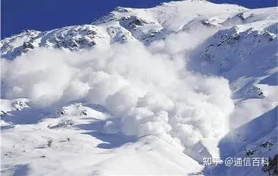
From this we can see that for an avalanche to occur, one condition is that the mountain must be high enough. Therefore, the avalanche photodiode adds an avalanche region to the basic structure of the PIN photodiode. This causes the impact ionization effect of photo-generated carriers in its depletion region (high-field region) to excite new electron-hole pairs. The newly generated carriers are accelerated by the electric field, leading to more impact ionization, one producing two, two producing three, and so on, thereby achieving avalanche multiplication of the photocurrent.
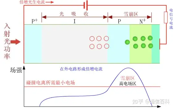
APD avalanche photodiode
Principle:
(1) Photons illuminate the semiconductor material to generate photo-generated carriers;
(2) The photo-generated carriers undergo avalanche multiplication in the avalanche region, i.e., the high-electric-field region;
(3) The photocurrent forms an electrical signal under the action of the external circuit and is output.
Finally, in actual work or engineering projects, we may focus more on certain important indicators of the photodetector, such as receiver sensitivity and overload point, which we will discuss next time.

Related Reading
- Lumentum’s Three-Step Mesa Structure APD
- Huawei: Strained-Layer C+L Band 100G Germanium-Silicon Photodetector
- Basics: Waveguide Photodetectors
Enjoy this article?
Subscribe to get new optical communication insights delivered to your inbox. Free, unsubscribe anytime.