This 2.5-minute video uses a slide deck to explain three key points about NPO (Near-Packaged Optics): why NPO is needed, the two schemes of multimode and single-mode, and how the package layout is arranged.
Why NPO?
In the conventional approach, the pluggable optical module is mounted at the panel edge, and the electrical signal has to travel more than ten centimeters on the PCB: insertion loss is high, the signal is distorted, and I/O power consumption is very high. To compensate for these losses, a high-power Retimer has to be added, along with expensive ultra-low-loss board materials – so neither cost nor power consumption can come down.
The Idea of NPO
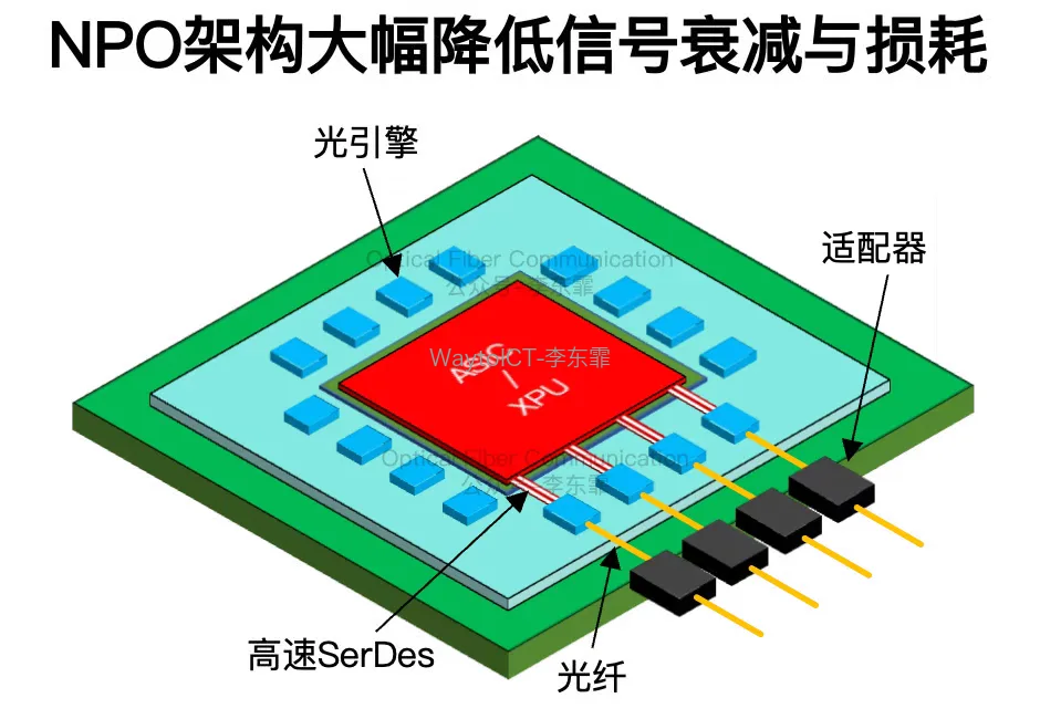
The idea of NPO (Near-Packaged Optics) is simple: move the optical engine from the panel edge to next to the ASIC chip, so that the electrical signal only travels a few centimeters or even a few millimeters, eliminating the series of problems caused by long routing.
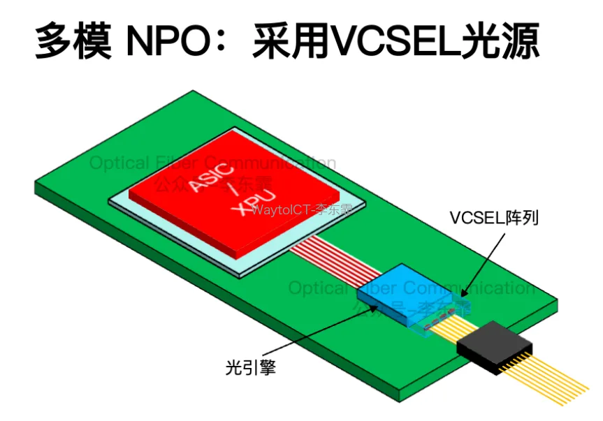
Multimode Scheme: Direct VCSEL Modulation
By light source, NPO is divided into multimode and single-mode categories. The multimode scheme uses a VCSEL array as the light source, directly integrated inside the optical engine. The VCSEL itself is a directly modulated light source – by changing the injection current, high-speed optical signals can be directly modulated. The structure is simple and the cost is low, but the transmission distance is relatively short.
Single-Mode Scheme: External Light Source + Silicon Photonics Modulation
In the single-mode scheme, the laser is separately packaged as an ELSFP module, providing continuous-wave (CW) laser light to the optical engine through a polarization-maintaining fiber array. After the laser light enters, the silicon photonics modulator inside the optical engine modulates the electrical signal onto the light: either using a microring MRM or a Mach-Zehnder MZM.
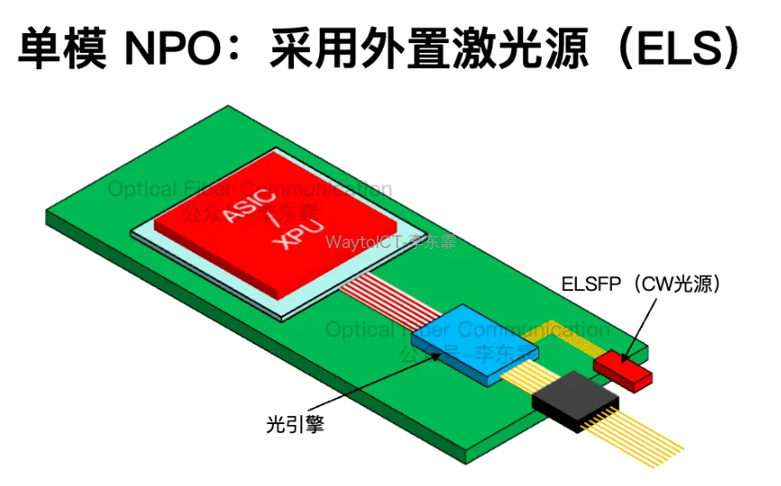
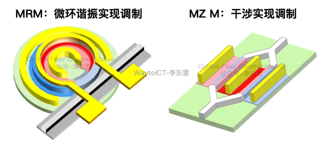
The external light source has another benefit: the ELSFP and the optical engine are physically separated, so the heat of the laser does not interfere with the optical engine; if it fails, it can also be hot-swapped at the panel to directly replace the module.
Package Layout: Horizontal and Vertical
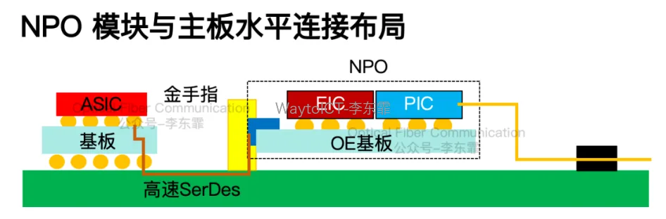
In terms of packaging, the industry recommends reusing mature gold-finger standards such as QSFP-DD and OSFP, making the NPO optical engine into the form of a pluggable module.
There are two kinds of connection layouts with the mainboard. The first is the horizontal layout: the module is parallel to the mainboard, tiled around the main chip, with a mature process, but it occupies planar space. When planar space is insufficient, use the already mature double-layer connector to stack two layers vertically, keeping the width unchanged and directly doubling the number of optical channels.
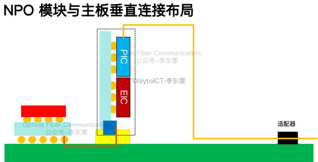
The second is the vertical layout: the module is inserted upright perpendicular to the mainboard, saving space around the main chip, but it has requirements on the vertical height of the cabinet.
Summary and Comparison
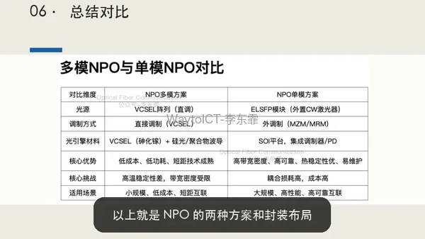
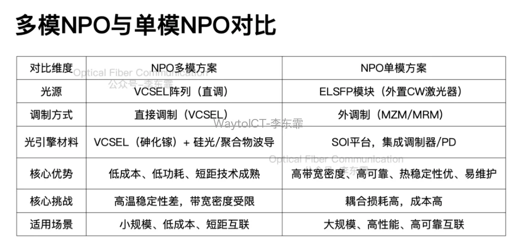
The multimode scheme: direct VCSEL modulation, low cost and low power consumption, suitable for small-scale, short-distance interconnection. The single-mode scheme is exactly the opposite: external ELSFP plus a silicon photonics modulator, offering high bandwidth, high reliability, and easy maintenance, suitable for large-scale high-performance interconnection. How to choose depends on your scenario and budget.
The video is produced by this site, narrated by Li Dongfei. To see the details of a particular section, just drag the progress bar.
Related Reading
- Basics: NPO Multimode and Single-Mode Schemes and Package Layout
- How Was the Path from OTN to Flexible FlexO Packaging Multiplexing Walked?
- What Are the Packaging Processes of Optical Modules?
Enjoy this article?
Subscribe to get new optical communication insights delivered to your inbox. Free, unsubscribe anytime.