Someone in our community asked about “wafer thinning and CMP.” On the surface, CMP also has a thinning effect, but they are actually quite different. In addition, there is also a grinding/polishing process that may cause some misunderstanding. Let us talk about them together below.
To more intuitively show the differences among these processes, let us first look at their positions in the manufacturing flow. I drew a schematic including part of the flow, as follows.
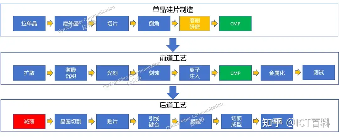
In the figure, the yellow background is the grinding/polishing process, the green background is the CMP planarization process, and the red background is the thinning process. It can be seen that their order in the flow differs: grinding/polishing comes first, then CMP (repeated multiple times), and finally thinning. For the CMP planarization process, you can first read my earlier article: Why Is the CMP Process Needed? Planarization CMP is used more frequently—on the silicon surface after ion implantation, on each metallization layer, and for polishing the top metal, etc. Grinding/polishing, on the other hand, mainly aims to reduce the thickness of the silicon wafer. Note that grinding and polishing are actually two concepts, usually performed in order from coarse to fine, that is, grinding first, then polishing. Grinding achieves the desired size or shape, while polishing removes the scratches and surface defects left by grinding—it is that simple. In addition, a special note: grinding grinds the back of the wafer, while polishing polishes the entire wafer, mostly the front side, and is mostly a physical method. As for CMP, let me mention again that CMP planarization is performed after each metal deposition and etching, using chemical etching and mechanical grinding. During wafer manufacturing, CMP may need to be performed multiple times, mainly concentrated on the front of the wafer. Finally, the thinning process—as the name suggests—has a simple purpose: to reduce the overall thickness of the wafer, thereby improving integration density, reducing thermal resistance, and meeting packaging requirements. This operation is a one-time operation on the entire wafer after all front-side manufacturing steps are completed, but before the wafer is diced into individual chips.
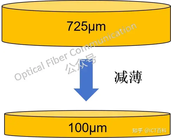
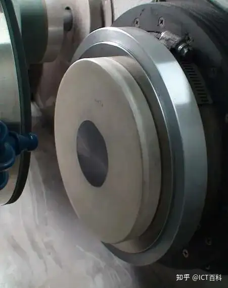
Therefore, it can be seen that the thinning process is different from the CMP process, and also different from the polishing mentioned above—it is more like grinding. Usually we use a grinding wheel containing diamond abrasive grains to grind at a certain speed, as shown in the figure below:
Let me draw another schematic of grinding-wheel thinning. My drawing may not be very good.
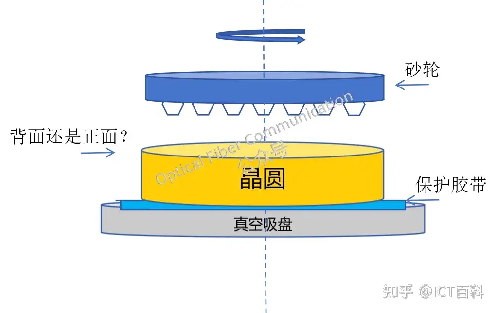
Finally, a small question: which side of the wafer is thinning performed on—the back or the front? Feel free to leave a comment! Thank you for reading!
Published with the permission of OFC!
Related Reading
- Why Is the CMP Process Needed?
- What Is Strained-Layer Epitaxy?
- Structure and Principle of Common Dry Etching Equipment for MEMS
Enjoy this article?
Subscribe to get new optical communication insights delivered to your inbox. Free, unsubscribe anytime.