A laser is a high-frequency (10¹³~10¹⁵ Hz) electromagnetic wave, whose amplitude, frequency, phase, and intensity can all be controlled and varied. By making any one of these parameters change according to the modulation signal, information can be loaded onto and transmitted by the laser. Through the modulation process, low-frequency information such as speech, text, and images is loaded onto the laser, where the laser serves as the carrier.

The low-frequency signal that controls its variation is called the modulation signal, and the device that completes this process is called the modulator.
According to the relative relationship between the modulator and the laser, optical modulation can be divided into internal modulation and external modulation.
Internal modulation loads the modulation signal during laser oscillation, changing the laser’s oscillation parameters to control the output characteristics. Its core is to apply the modulation signal directly to the laser itself.
Specifically, there are two implementation approaches:
- One is to place a modulation element inside the laser resonant cavity, using the modulation signal to control the physical-property changes of the element, thereby adjusting the cavity parameters and changing the laser output characteristics;
- The other is for injection-type semiconductor lasers, where the modulation signal directly controls the pump current, making the output laser intensity change correspondingly with the current. This intensity modulation achieved through the drive current is also called direct modulation.
Both approaches complete information loading by changing the laser’s internal parameters, forming a complete internal-modulation technology system.
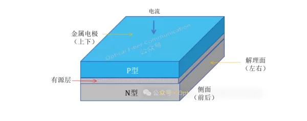
The schematic below shows the basic structure of a fundamental semiconductor laser, a sandwich structure composed of a thin active layer about 0.1 micrometers thick, a P-type semiconductor layer, and an N-type semiconductor layer.

Among these, the active region also functions as an optical waveguide, using the natural cleavage planes of the crystals at both ends to form a mirror structure, together constituting a rectangular dielectric optical-waveguide resonant cavity, achieving laser amplification through optical oscillation within the cavity. After the operating current is injected into the active region through the electrodes, it induces population inversion and triggers electron-hole recombination, ultimately producing coherent light output through stimulated emission.
External modulation is a technique that controls optical parameters through an external modulator after the laser is formed. Its principle is to use the modulation signal to change the physical properties of the modulator, causing the amplitude, frequency, or phase of the passing laser to vary in a controlled manner. By operating principle, it can be divided into electro-optic, acousto-optic, and magneto-optic modulation; by signal-loading method, it is divided into amplitude modulation, frequency modulation, phase modulation, and intensity modulation.
The figure below shows external modulation that uses the flat-dispersion property at the band edge of a photonic crystal waveguide to reduce the phase-shift modulation length of the device.

Compared with internal modulation, external modulation has the advantages of convenient operation, higher modulation rate (about an order of magnitude higher), and wider bandwidth, making it suitable for high-precision optical communication.
Welcome to purchase our knowledge base, which collects core ICT technical documents, covering a complete knowledge system from basic theory to cutting-edge applications.
When purchasing, please first note the intended <username>, with the first letter capitalized. We will create the account accordingly and then send the default password to you via shipment.
Related Reading
- Why Do Semiconductor Lasers Need a Narrow Linewidth?
- What Is EML? The Working Principle, Applications, and Evolution of Electro-Absorption Modulated Lasers (EML)
- How Much Bandwidth Gain Does Increasing the Modulation Order Add?
Enjoy this article?
Subscribe to get new optical communication insights delivered to your inbox. Free, unsubscribe anytime.