
Published with the permission of the WeChat official account “Optical Fiber Communication.”
To achieve more functionality and higher performance, we build layer upon layer of wiring on the chip. This is what we often call multi-layer interconnect technology.
But at the same time, it brings a challenge: each additional wiring layer is like stacking bricks on originally smooth ground, making the chip surface bumpy and uneven. Such an uneven surface not only affects the efficiency of current transmission but may also cause a series of defects and failures, posing a considerable threat to subsequent manufacturing processes.
Therefore, how to flatten these layers has become an urgent problem in chip manufacturing. And the CMP process is exactly the key to solving this problem. First, let us talk about the historical background of the CMP process. With the development of system-level LSIs and advanced CMOS digital circuits, the trend toward multi-layer interconnection has become increasingly evident. Multi-layer interconnection is like building skyscrapers on a chip—the higher the floors, the more a solid foundation and flat ground are needed. And the CMP process is the “engineer” that builds the solid foundation for this “chip skyscraper.”
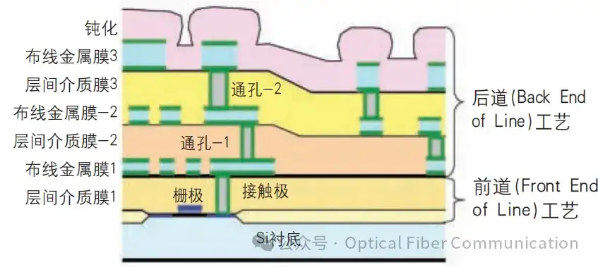
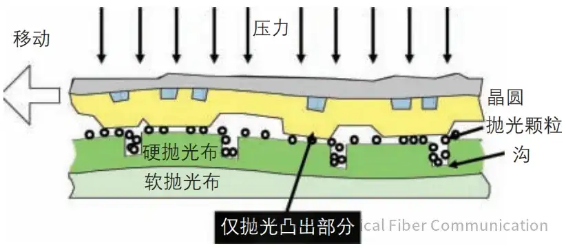
In memory devices, because the structure of memory cells is relatively simple, usually only two layers of bit-line and word-line wiring are needed, so the CMP process is sometimes not required. But in more complex digital circuits, the situation is completely different. To quickly complete the design and verify its reliability, we usually adopt the Building Block approach, combining already-verified circuit modules like building blocks. In this way, the wiring necessarily forms a hierarchical structure, requiring multi-layer interconnection. And the surface-unevenness problem brought by multi-layer interconnection needs the CMP process to solve. CMP mainly uses the dual action of chemical etching and mechanical polishing to flatten both the bumps and depressions on the wafer surface, making it as smooth as a mirror. In this way, current can flow more smoothly, improving chip performance. At the same time, a flat surface also reduces defects and failures, improving chip reliability.
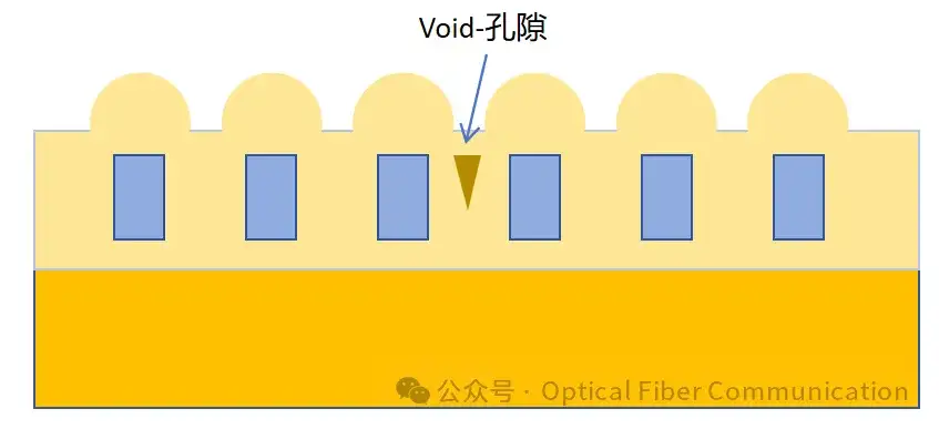
In fact, before the CMP process became practical, people had already tried other planarization techniques. But from the 1980s to the 1990s, these techniques all faced some difficulties. For example, as wiring width and spacing shrank, the interlayer dielectric film could hardly completely fill the gaps between wiring, causing “Void” pores to appear, which seriously affected chip reliability. To solve this problem, gap-fill technology was invented. However, although this technology could solve part of the problem, it could not fully achieve surface planarization.
Besides surface planarization, how to planarize the wiring steps is also a big problem. Although there are some techniques, such as coating-type interlayer dielectric smoothing and lithographic etch-back, none of these methods can achieve complete planarization. The existence of wiring steps not only affects the efficiency of current transmission but may also cause a series of manufacturing problems.

Here, we need to know that the combination of chemical etching and mechanical polishing is the best planarization technique for reducing the absolute height of steps. On the other hand, our lithography machines also need CMP technology, as a key piece of equipment in chip manufacturing. If the chip surface is not flat during lithography, it will cause distortion and deformation of the lithographic pattern, affecting chip function and performance. By planarizing the chip surface with the CMP process, the accuracy and consistency of the lithographic pattern can be ensured, improving chip-manufacturing yield and reliability. In addition, in CMOS circuit manufacturing, the CMP process also plays an irreplaceable role. CMOS circuits have a complex structure and many wiring layers, so the surface-unevenness problem is particularly prominent. By planarizing the CMOS circuit surface with the CMP process, defects such as wiring steps and pits can be eliminated, improving circuit stability and reliability. It can be said that without the CMP process, devices could not be manufactured.
Related Reading
- What Is Wafer Thinning, and How Does It Differ from CMP and Grinding?
- What Is Strained-Layer Epitaxy?
- Structure and Principle of Common Dry Etching Equipment for MEMS
Enjoy this article?
Subscribe to get new optical communication insights delivered to your inbox. Free, unsubscribe anytime.