In fields such as antennas/electromagnetic waves and signal processing, we often encounter a phenomenon called the skin effect.
What is the “skin effect”?
In plain terms, when the signal frequency is very high, current prefers to flow along the surface of a conductor rather than uniformly through the entire material. As a result, the middle part of the conductor barely participates in conduction, and only the surface is busy.
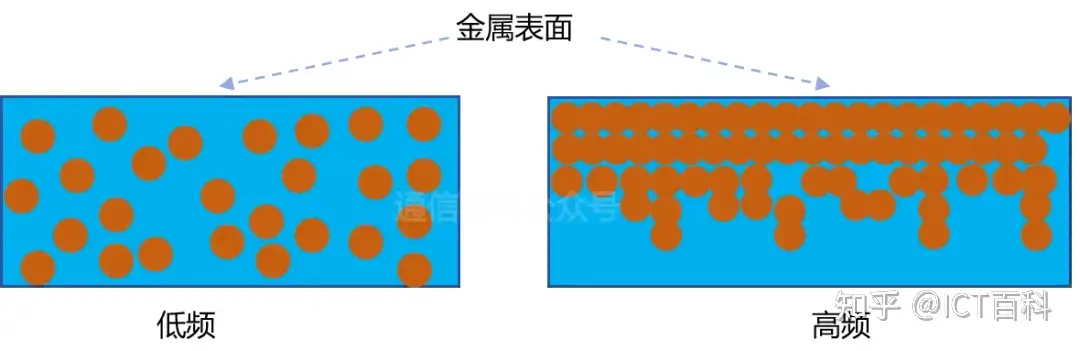
I wonder if any of you have ever swum in a flowing river. Near the water surface, you can feel the water flowing fast, but when you dive into deeper water, the current seems to weaken. This is somewhat similar to the skin effect.

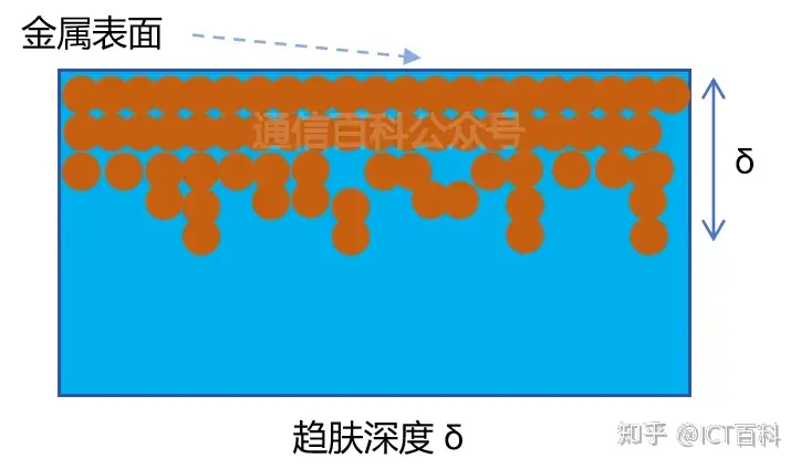
To accurately describe the skin effect, the concept of “skin depth” was introduced, which describes the thickness within which the current flows only on the surface, and is also the effective thickness of the transmission path.
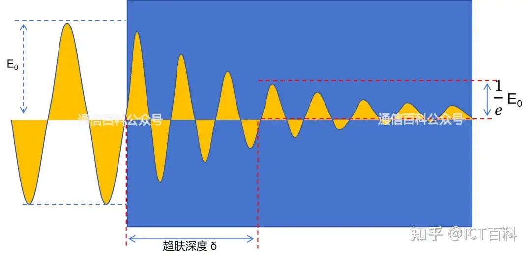
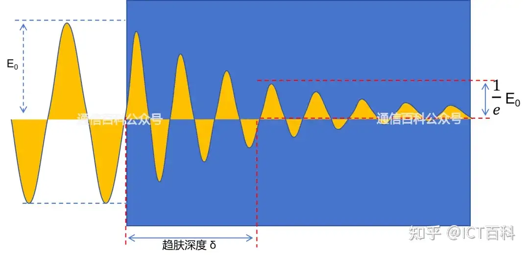
Specifically, if we consider an electric field with an initial amplitude E₀ in free space, when it penetrates into the interior of a good conductor, its amplitude begins to decrease gradually. The specific distance the electric field penetrates into the conductor, at which point the electric field amplitude drops to 1/e of its initial value, that is, 36.8% of the original field strength, is what we call the skin depth.
The skin depth δ is usually calculated by the following formula:
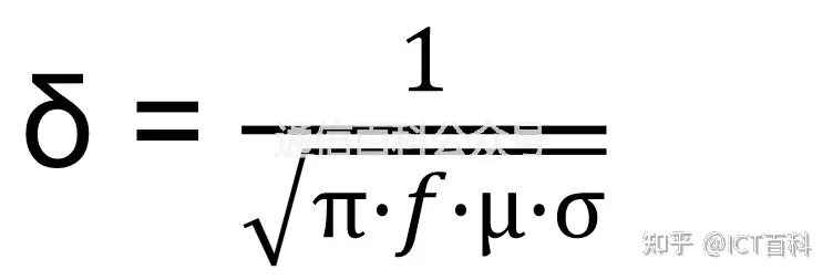
Among them, f is the frequency, σ is the conductivity. And δ here refers to the depth at which the electric field strength attenuates to 1/e.
Under DC, the frequency is 0 Hz, and according to the formula, it can be simply understood that δ is infinite, meaning the entire conductor is conducting. But at high frequencies such as microwaves, the higher the frequency f, the more the current concentrates on the surface. The current density gradually decreases from the surface inward, and at a certain depth, the current is almost zero.
The figure below describes the conduction of an RF signal, with red representing the maximum current density and blue representing no RF signal.

Therefore, when designing microstrip lines or other high-frequency circuits, we must pay special attention to the influence of skin depth on material selection and conductor size design. For example, the thickness of the conductor should be chosen based on the skin depth. If the thickness is chosen too thick, it not only wastes material but also does little to reduce loss.
Thank you for reading!
Welcome to join our community, with massive resources continuously updated for 900+ days!

Related Reading
- Probabilistic Constellation Shaping PCS (2)
- For Data Center 800G, PAM4 or Coherent Technology?
- Light and Technology: What Is the Story Behind Nonlinear Effects in Optical Fiber?
Enjoy this article?
Subscribe to get new optical communication insights delivered to your inbox. Free, unsubscribe anytime.