Before we begin, we first need to understand the concept of “layer” in a chip.
Chip design adopts a layered approach, corresponding to different functional structures in the manufacturing process. For example, the pattern layers in the mask, and the material layers on the wafer (such as metal layers, polysilicon layers, and dielectric layers).
Among these, the PCB circuit layout is the final result of our chip design. The circuit layout is the physical expression of the chip design, and each of its layer designs (such as the metal interconnect layer) corresponds to one mask. Through the lithography process, the mask pattern is transferred onto the silicon wafer, forming the actual physical layer.
As shown on the left of the figure below, the transistor design layout is taken from part of the circuit layout.

Different colors represent different layers, which also correspond to the corresponding masks. After lithography, each mask forms a material dielectric layer on the wafer. Each layer design in the circuit layout (such as the metal layer and polysilicon layer) corresponds to one mask, and however many layers the circuit layout has, that is how many material dielectric layers there will ultimately be on the wafer.

These material dielectric layers are stacked on the silicon wafer, forming all the circuit components and circuit interconnects across the entire chip, and even across the entire silicon wafer, which is called the circuit layer. It should be made clear here: a single bare die itself already contains a complete multi-layer circuit structure (such as the transistor layer and metal interconnect layer). It is not the case, as some places say, that a bare die has only one circuit layer.
There are no more components stacked on top of these components. After circuit-layer manufacturing, dicing, packaging, and testing, our traditional 2D chip is formed.
In a 2D chip, multiple dies are laid flat on the silicon wafer, referring to a single package without stacking.

We add a silicon interposer layer dedicated to wiring between the circuit layer and the package substrate of the 2D chip. The dies are stacked onto the interposer, and the silicon interposer achieves vertical interconnection between the chip and the substrate through TSVs. Such a chip is called a 2.5D chip.

It should be noted that in a 2.5D chip, the dies themselves are not vertically stacked.
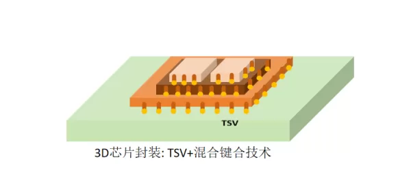
A 3D chip, on the other hand, refers to multiple circuit layers stacked together, with a circuit layer on each die. But unlike the 2.5D chip, in 3D packaging, TSVs directly achieve vertical interconnection of multiple silicon-wafer layers on the chip. As shown in the figure below:

Let us make an analogy: a 2D chip is like a single-story bungalow; 2.5D is like a duplex with a loft (interposer = stairs); 3D packaging is like a multi-story apartment.
Here let us mention memory chips. Although their package shell contains a single die, if many circuit layers are integrated on this die, then the memory chip can also be regarded as a 3D chip. In 2021, Micron launched a 176-layer 3D NAND flash chip.
However, it should be noted that 3D NAND is the vertical stacking within a single die (belonging to chip manufacturing processes), while 3D packaging is the vertical stacking of multiple complete dies (belonging to packaging technology). The two are still different in terms of hierarchy.
Thank you for reading. If there are any inaccurate statements, please point them out~
Related Reading
- CPO and 2.5D/3D Advanced Packaging
- How Did the Packaging and Multiplexing Path from OTN to Flexible FlexO Evolve?
- What Packaging Processes Are There for Optical Modules?
Enjoy this article?
Subscribe to get new optical communication insights delivered to your inbox. Free, unsubscribe anytime.