Sharing some views from TSMC’s Dr. Lu on advanced technology design approaches.
Dr. Lu joined TSMC in 2000 and has headed the Design and Technology Platform division since 2018. Working with the process R&D team, he developed design-technology co-optimization (DTCO).
We have discussed DTCO in a previous article, “Acacia/Cisco: DTCO and STCO Co-Optimization Approaches for High-Speed Optical Modules.”
Dr. Lu’s views mainly revolve around three key points: advanced DTCO, packaging innovation, and AI design methods. The core view is that in the era of AI and high-performance computing, design must be deeply bound to the process, combined with system integration, for Moore’s Law to continue advancing.
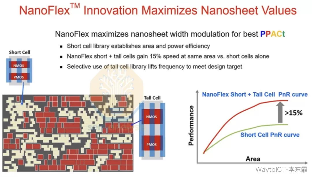
On the device and design side, TSMC relies on DTCO and DDCL to advance from N5 to N2 and then to A14. NanoFlex and NanoFlex Pro optimize standard-cell design and improve energy efficiency. Compared with conventional cells, N2’s NanoFlex achieves up to a 50% speed increase at the same voltage, and up to a 50% power reduction at the same performance.
A14’s NanoFlex Pro adopts a merged-oxide-diffusion-layer architecture with 1.5x cell height, achieving higher interconnect-layer utilization with compact arrangement of high- and low-speed cells. Compared with N2, speed improves by 10% to 15% and area shrinks by about 20%. One process generation achieves cross-generation gains.
N2P and N2U continue to optimize DTCO and power-delivery schemes. The hybrid dual-rail architecture lowers the minimum operating voltage by more than 200 mV, reducing energy consumption by about 40%. N2U improves performance by 3% to 4% over N2P, or reduces power consumption by 8% to 10%, and is compatible with existing design rules and IP, making customer migration almost imperceptible.
After process and cell optimization, EDA tools must also keep up. TSMC works with EDA vendors to complete tool adaptation, and the AI design flow has landed. Agent AI runs throughout the entire flow, responsible for placement, routing, and performance tuning, balancing efficiency and quality. Analog and RF design also use this approach, enabling faster cross-process migration and shorter time-to-market.
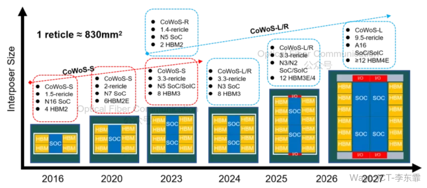
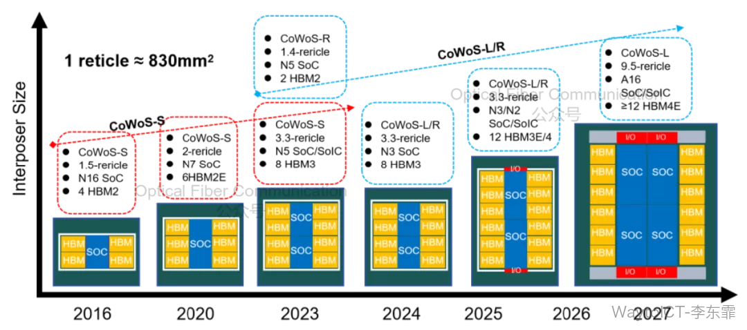
In system-level packaging, CoWoS, SoIC, and 3D Fabric are the main forces for expanding AI computing power. CoWoS mask size and integration scale continue to expand, greatly improving computing density.
From 2024 to 2029, the transistor count of a single CoWoS system is expected to grow 48-fold, thanks to packaging expansion, increased chip integration, and new processes such as A14.
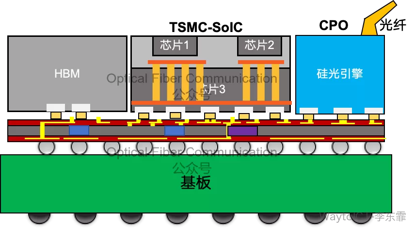
While computing power increases, memory bandwidth must also keep up. HBM stack layers are developing from 8 layers to 24 layers, single-stack I/O bandwidth doubles, and overall bandwidth grows 34-fold. Behind this are DRAM technology iterations and advanced-process logic base-die upgrades.
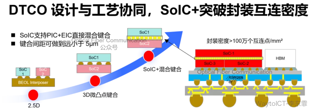
The key to 2.5D/3D integration is micro-bump pitch scaling. CoWoS shrinks bump pitch to improve bandwidth density and energy efficiency. SoIC bump pitch drops to about 4.5 micrometers, improving bandwidth density 4-fold with significantly lower power consumption.
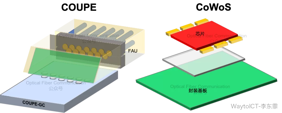
TSMC: CPO evolution roadmap based on COUPE and CoWoS packaging. The COUPE optical engine integrates silicon photonic technology, with optical interconnect improving energy efficiency by 5 to 10 times over electrical interconnect and reducing latency by 10 to 20 times.
However, the increase in computing density brings power-delivery and heat-dissipation challenges. For power delivery, MIM capacitors and eDDC increase capacitance density by more than 10 times, effectively suppressing voltage fluctuation. For heat dissipation, optimizing packaging materials and structures reduces thermal resistance by up to 40%, ensuring stable operation under high load.
Finally, to summarize, TSMC is pushing two things: 3D IC design standardization and AI-automated design. The new “3D module” design system simplifies the 3D IC R&D process, makes ecosystem collaboration smoother, and promotes IEEE standards. Combined with generative AI and agent optimization technologies, it can greatly improve the efficiency and scalability of chip and package co-design.
Recommended Reading
- TSMC: Silicon Photonic Device Performance and Process Platform for CPO
- TSMC: CPO Packaging Flow Based on Silicon Photonic TDV Process
- Samsung: Latest Performance and Evolution Roadmap of the CPO Silicon Photonic Platform
- STMicroelectronics: Progress of the Silicon Photonic Process Platform Supporting NPO/CPO
Thank you for reading.
Please point out any inaccuracies.
The optical chip, optical device, and optical module (OFC2026) report compilation, color-printed and A4-bound, in two volumes totaling about 525 pages and about 200,000 characters. If you need it, welcome to contact us to order; the price is affordable!
Enjoy this article?
Subscribe to get new optical communication insights delivered to your inbox. Free, unsubscribe anytime.