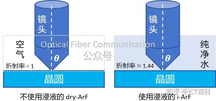
In the development of semiconductor manufacturing, lithography is known for its persistent pursuit of Moore’s Law. This technology follows the mathematical model of the Rayleigh criterion, namely:
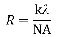
Here R is the resolution, k is the process factor, lambda is the exposure wavelength, and NA is the numerical aperture. Let us briefly discuss these factors: exposure wavelength lambda – for 0.1um to 90nm processes a 193nm light source is used, generally the smaller the better.
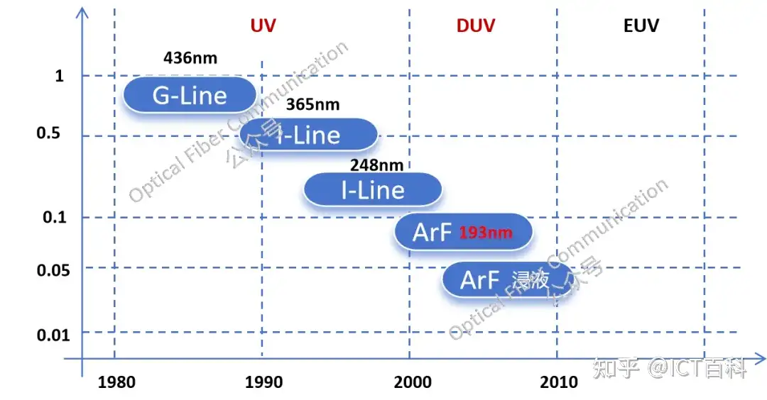
Process factor k: usually between 0.25 and 0.5, depending on the complexity of the lithography process and the required imaging quality, the smaller the better; numerical aperture NA: the numerical aperture of the lens, the larger the better. Through continuous optimization of the above parameters – especially reducing lambda, increasing NA, and working with photoresist processes to lower the k factor – lithography can achieve higher resolution at a given wavelength. For example, at a wavelength lambda of 193nm, using ArF (argon fluoride) dry lithography, mass production of 65nm semiconductors can be achieved.
From the formula, the shorter the wavelength, the finer the lithography. To achieve even higher resolution, can we not continue to reduce the wavelength lambda? In this regard, based on the output wavelength characteristics of fluorine gas excimer lasers, engineers considered 157nm as an option for the next-generation exposure wavelength. However, light of this wavelength has insufficient penetration, requiring improvements in photomask and lens technology. At the same time, because oxygen absorbs light at this wavelength, non-absorbing gases such as nitrogen must be used instead to avoid absorption problems in the medium. Therefore, 157nm lithography did not become mainstream.
So what to do?
At this point, ASML and TSMC took a different path and proposed: must we really stick to a dry medium?
TSMC discovered that after 193nm light is refracted through water, its wavelength becomes 132nm, directly skipping the 157nm wavelength. This is the basic principle of immersion lithography – the exposure medium is water, and its exposure equipment is called i-ArF. At the time, compared with the dry medium, the potential of immersion ArF lithography could leap across technology nodes from 45nm to 32nm and even 22nm.
PS: Let me briefly explain what a dry medium is. Simply put, it means that no liquid medium is used in the lithography machine; gas is used instead. For example, ArF (argon fluoride) dry lithography directly uses air, and its exposure equipment is called dry-ArF (d-ArF).
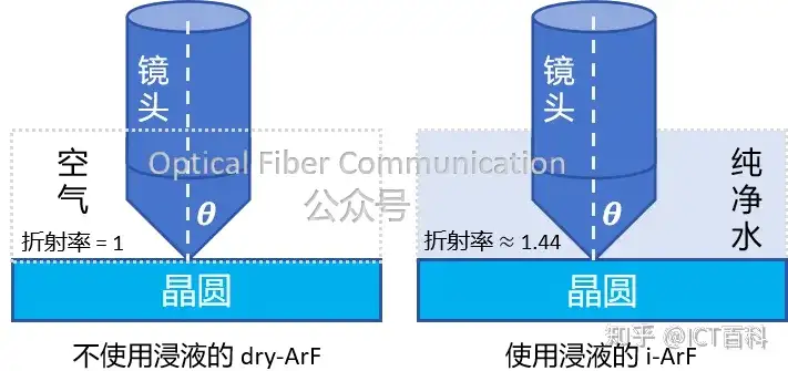
In immersion lithography, it may appear that we are shortening the wavelength, but in fact we are only using the law of refraction of light: the wavelength of light is equivalently shortened because of the presence of the liquid. Essentially, it is still increasing the numerical aperture NA, which is also related to the refractive index of the medium.
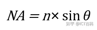
Combining with the figure above, the refractive index of water is about 1.44. When theta (the angle at which light enters the edge of the optical system’s aperture) is greater than 70 degrees, the numerical aperture NA is greater than 1. Here we might wonder: is a larger NA always better? In theory, the larger the NA, the higher the resolution of the lithography machine and the smaller the feature size that can be manufactured. But in practice this is not the case. As NA increases, another problem emerges, namely the limitation brought by depth of focus (DOF).
Depth of focus refers to the allowable range within which the wafer can deviate from the ideal focal position relative to the lithography machine lens during the lithography process.
The formula for depth of focus and numerical aperture NA is as follows:
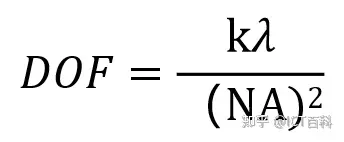
A larger depth of focus means a clear image can still be maintained within a larger range of vertical deviation. From the formula above, DOF is inversely proportional to the square of NA. As NA increases, DOF decreases rapidly – that is, the allowable range within which the lithography lens can deviate from the ideal focal position becomes smaller and smaller. In other words, as NA increases, resolution improves, but depth of focus shrinks. The shrinking depth of focus in turn imposes higher requirements on wafer flatness and alignment accuracy. For flatness (CMP), refer to: Why is the CMP process needed?, What is thinning, and how does it differ from CMP, grinding, and polishing?
One cannot help but wonder: what is the limit of immersion? In my view, the earlier talk of developing immersion liquids with higher refractive index may not be the correct technical route.
Finally, let us briefly talk about products based on immersion lithography:
At the end of June 2005, Nikon released its advanced lithography system “NSR-S690B”. This system’s numerical aperture (NA) reached 1.07, capable of mass production at the 55nm node and R&D lithography requirements at the 45nm level. Right after Nikon’s release, ASML released its immersion lithography system “XT:1700i” in early July 2005, with an NA as high as 1.2, supporting the 45nm lithography process.
It is worth noting – and this also answers the question above (what is the limit of immersion?) – that the pursuit of even smaller feature sizes has exceeded the physical limits of immersion lithography. Therefore, extreme ultraviolet (EUV) lithography was developed to achieve even smaller feature sizes, such as the 7nm, 5nm, 3nm, and even smaller process nodes.
Thanks for reading!
Related Reading
- New EUV Photoresist
- How Are Photoresist Patterns “Copied” onto Chip Materials?
- Do You Know These Properties of Photoresist?
Enjoy this article?
Subscribe to get new optical communication insights delivered to your inbox. Free, unsubscribe anytime.