The Tomahawk 5 (BCM78900 series, abbreviated TH5) chip launched by Broadcom is a breakthrough product designed for next-generation data centers and AI/ML networks. This monolithic switch chip built on a 5nm process sets a new industry benchmark with a 51.2Tb/s switching capacity, doubling the bandwidth over the previous generation, while balancing high performance and low power consumption through multiple technological innovations.
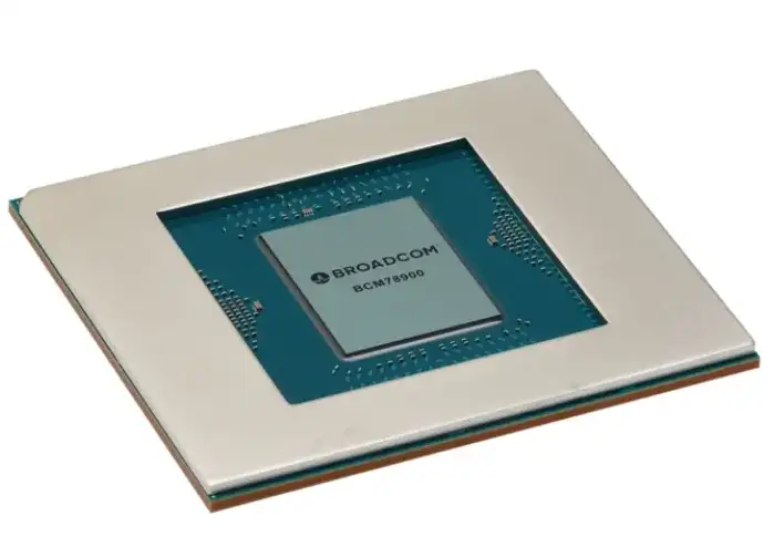
The core advantage of TH5 stems from its highly integrated architecture. The chip carries 512 106.25Gb/s PAM4 SerDes lanes, supporting flexible port configurations from 100GbE to 800GbE, and dynamically allocates resources through a shared-buffer architecture, significantly improving burst traffic handling capability and quality of service.
Broadcom’s self-developed Peregrine SerDes technology not only supports multiple physical connection schemes such as direct attach copper (DAC), linear pluggable optics (LPO), and co-packaged optics (CPO), but also achieves signal insertion loss performance of more than 45dB, providing data center operators with cost-effective networking options.
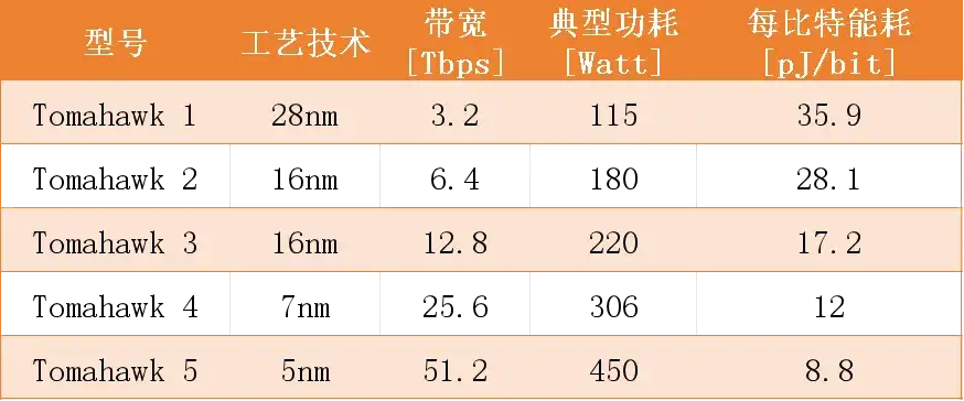
Power control is one of the core challenges in TH5’s design. Through multi-level adaptive voltage scaling (AVS) technology, the chip dynamically optimizes voltage distribution in the range of 0.7V to 0.7875V with 12.5mV precision. Combined with architectural innovations, the typical operating power consumption is ultimately reduced to 450W, further reducing the energy per bit from 12.0pJ of the previous generation to 8.8pJ.
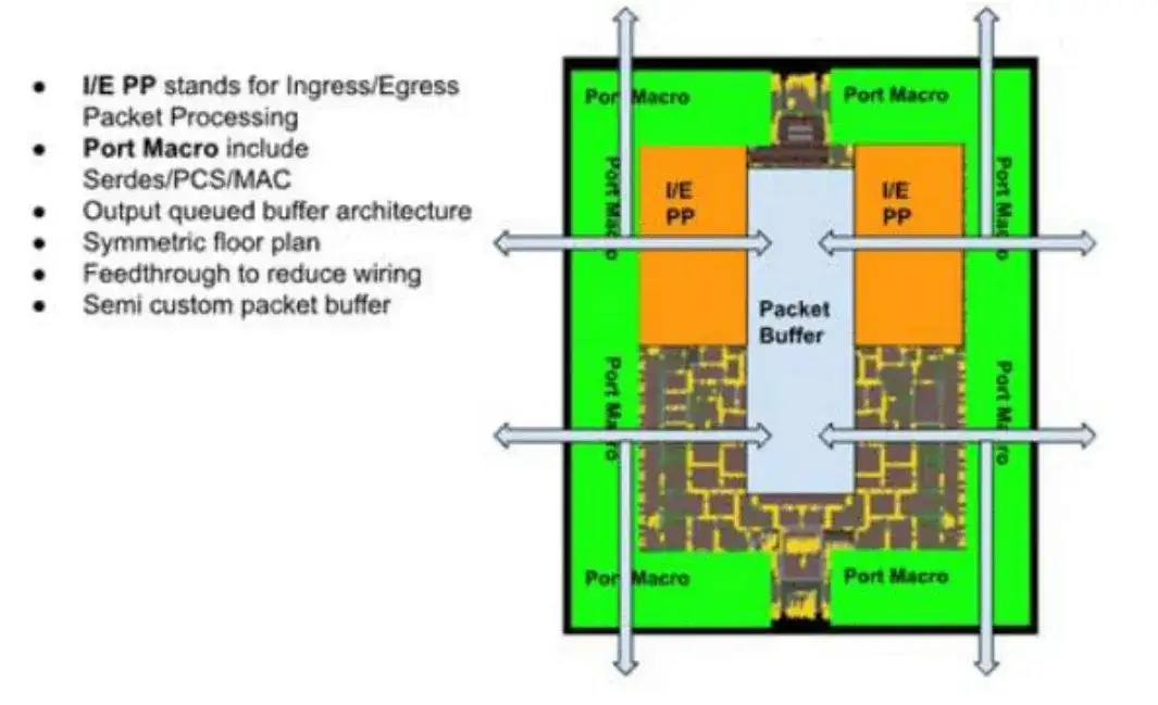
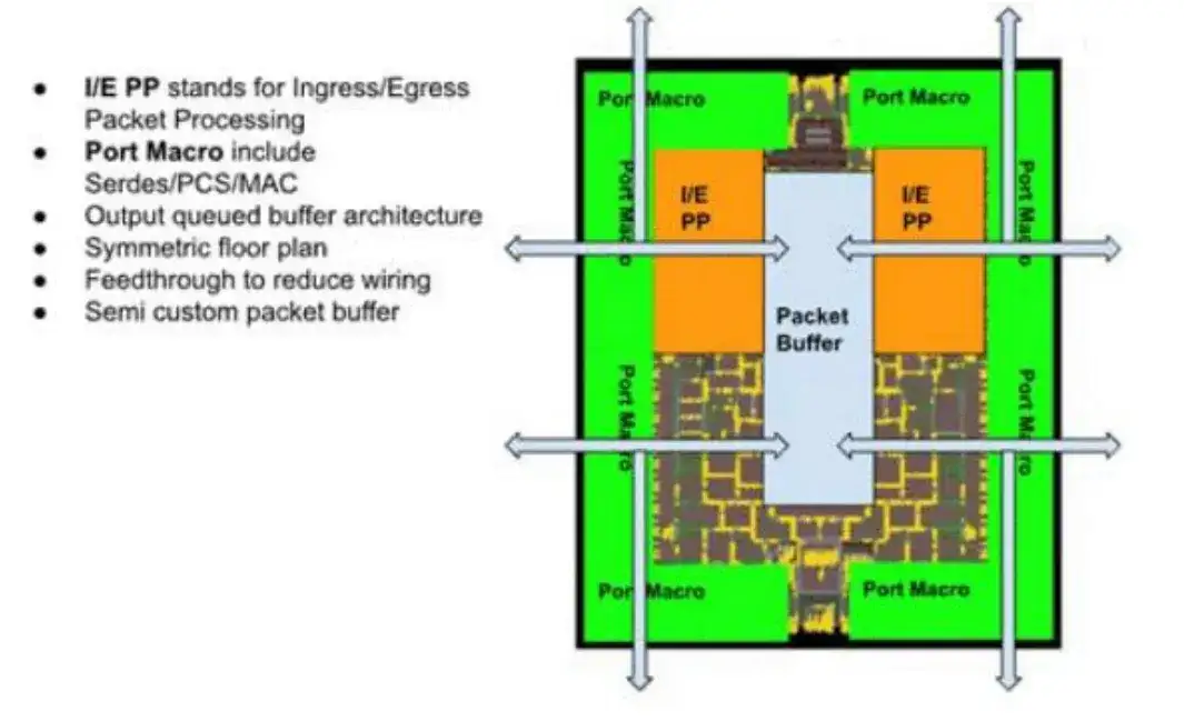
This achievement benefits not only from the energy efficiency improvement of the 5-nanometer process, but also from the synergistic improvement of microarchitecture optimization and SerDes technology. For example, TH5 adopts a symmetric layout design to reduce the number of physical modules, improves memory utilization through semi-customized packet buffering, and uses feed-through wiring to lower interconnect cost.
In addition, the chip’s power delivery network (PDN) design needs to cope with the extreme operating condition of a 430A current transient within 550 nanoseconds. To this end, the team used a combination of multilayer copper PCB and decoupling capacitors to strictly control voltage ripple within 3%, ensuring system stability.
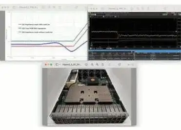
In terms of packaging technology, TH5 adopts an innovative compressed hexagonal BGA layout (ball pitch 0.9mm) (Fig. 16.1.4), reducing package size while optimizing signal integrity. Through a pre-configured customized test platform, Broadcom completed comprehensive verification of chip-package interaction effects before tape-out, ultimately passing the JEDEC component-level reliability test in one attempt and meeting stringent standards such as high-temperature warpage. In actual deployment, the TH5 validation kit (SVK) achieves efficient heat dissipation with a lidless package combined with an air cooling system (bottom of the figure above), supporting 64 800G ports interconnected through stacked OSPP connectors, showcasing a minimalist system design philosophy.
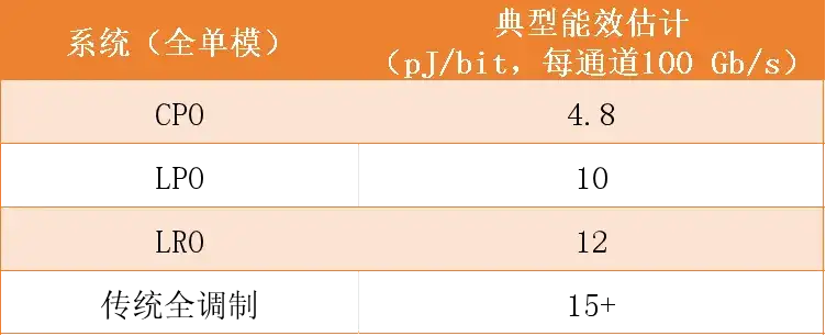
For optical module integration, TH5 supports co-packaged optics (CPO) solutions, achieving energy efficiency of 4.8pJ/bit (Fig. 16.1.5), saving more than 60% energy compared with traditional fully-modulated optical modules.
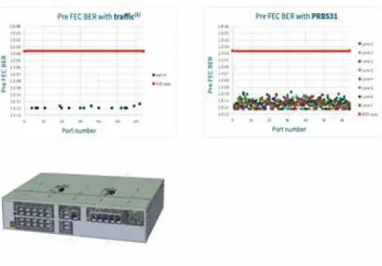
The link performance of the optical modules (as shown below) further verifies their reliability in complex scenarios. The upper-left part of the figure shows the pre-FEC bit error rate (Pre FEC BER) using the PRBS31 test pattern; the upper-right part shows the pre-FEC bit error rate (Pre FEC BER) under real traffic; and the bottom is its module test platform (MTP), used for LRO/LPO optical module validation.
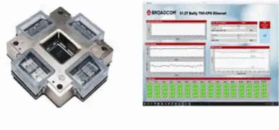
The left part of the figure below shows that Tomahawk 5 co-packages 8 optical engines, each with a capacity of 6.4T; the right part shows that the Tomahawk 5 co-packaged optical link performance complies with the IEEE 400GBase-FR4 standard.
From the perspective of technological evolution, the Tomahawk series started at 3.2Tb/s on the 28-nanometer process and, through five generations of iteration, has continuously broken through in process nodes, bandwidth density, and energy efficiency ratio.
Reference: IEEE – Tomahawk 5: 51.2Tb/s 5nm Monolithic Switch Chip for AI/ML Networking.
Together with several bloggers, we have built an ima Q&A tool in the ICT field, currently free to join – welcome to experience it:

Related Reading
- Ethernet and Optical Transport – FlexE (2)
- Introduction to 400G Ethernet Transceivers
- Flex Ethernet (FlexE) Link Interface Test Method (YD/T 3992-2021)
Enjoy this article?
Subscribe to get new optical communication insights delivered to your inbox. Free, unsubscribe anytime.