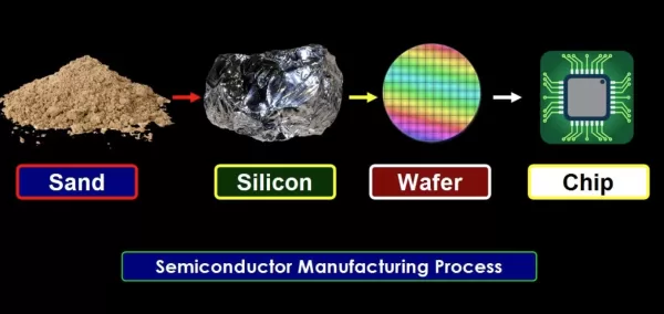
For silicon to become a semiconductor chip, it must go through several complex processes: wafer fabrication, oxidation, photolithography, etching, deposition and ion implantation, metal wiring, EDS, and packaging.
Let us take a detailed look at this important semiconductor manufacturing process.

- Wafer: the foundation of the semiconductor.
- Oxidation: forming an oxide film on the wafer surface.
- Photolithography: drawing the circuit design on the wafer.
- Etching: removing unnecessary material.
- Deposition and ion implantation: coating the wafer with thin films at the required molecular or atomic level.
- Metal wiring: making current flow by depositing a metal thin film.
- EDS: the testing process that ensures the semiconductor chip is flawless.
- Packaging: cutting the final wafer into individual semiconductor chips.
Now let us understand all the above steps in detail.
1. Silicon wafer fabrication – the foundation of all semiconductors
Semiconductors are stacked tall and solid, forming a complex structure like a high-rise building. A building starts from its foundation. Likewise, the silicon wafer is the foundation of the semiconductor.
Most silicon wafers are made from silicon extracted from sand. But have you ever wondered how these tiny grains of sand turn into silicon wafers?
First, the sand is heated until it melts into a high-purity liquid, then solidified through crystallization. The resulting silicon rod is called a silicon ingot. These ingots are cut into thin slices. The sliced wafers have rough surfaces and contain defects. Therefore, a polishing machine is needed to polish the wafer surface. The reason is that surface defects can negatively affect the precision of electronic circuits.
If you look at a photo of a silicon wafer, you will see a grid pattern on its surface. The wafer made in this way is the main material of semiconductors. The larger the diameter of the wafer, the more chips can be produced.

PS: Silicon is extracted from silica sand (also called quartz sand, white sand, or industrial sand).
2. Oxidation – forming an oxide film on the wafer surface.
The silicon wafer made in step 1 is not yet conductive. It must go through a process to become a semiconductor wafer. First, the wafer goes through the oxidation process. Oxygen or water vapor is sprayed onto the wafer surface to form a uniform oxide film.

This oxide film protects the wafer surface in subsequent processes and prevents current leakage between circuits. This thin film acts like a solid protective shield.
3. Photolithography – drawing the circuit design on the wafer
The so-called photolithography is also abbreviated as “photo”, because it resembles developing a photo taken with a film camera using a semiconductor.
The photomask acts as the film and is a glass substrate with computer-designed circuit patterns.

To draw circuits on the wafer, photoresist, a material that reacts to light, is thinly and uniformly applied on the oxide film previously placed on the wafer.
Now, when light passes through the patterned photomask, the circuit is drawn on the wafer surface. Just like developing a photo, by spraying, developing, and removing unexposed areas from the exposed areas, the circuit pattern is printed on the wafer.
After checking whether the pattern on the wafer is completely drawn, we move to the next step.
4. Etching – removing unnecessary material
Liquid or gas etching techniques are usually used to selectively remove all unnecessary material to draw the desired design pattern.
- Wet etching: when etching is done using a chemical solution, it is called wet etching.
- Dry etching: when etching is done using gas or plasma, it is called dry etching.

Let us imagine building a building on a semiconductor chip smaller than a fingernail and thinner than paper.
The photolithography and etching processes are repeated layer by layer many times on the wafer. Here, an insulating film is needed to separate and protect the stacked circuits. This is called a thin film. This process is very similar to the manufacture of multilayer PCB boards.
5. Deposition and Ion Implantation
Coating the wafer with the required molecular or atomic-level thin film is called deposition. Because the coating is very thin, precise and complex techniques are needed to uniformly apply the film to the wafer to give it semiconductor electrical characteristics. Ion implantation is also required.
Semiconductors made of silicon do not conduct electricity, but impurities are added. It can then conduct current and has conductive properties.

In short, through the processes of wafer fabrication, oxidation, photolithography, etching, deposition, and ion implantation, the wafer becomes conductive and countless circuits are drawn on it.
6. Metal Wiring
Now, for the circuit to work, electrical signals must be applied. A path for current to pass through must be created according to the circuit pattern. This process is called the metal wiring process.
This is a process of making current pass through semiconductor holes by depositing a thin metal film using materials such as aluminum, titanium, or tungsten.

PS:
- Although copper has about 40% lower conductive resistance than aluminum, its use is avoided in semiconductor manufacturing.
- Copper is considered a semiconductor killer. It can rapidly diffuse into silicon, changing the electrical characteristics of silicon and preventing transistors from working properly.
- Aluminum is the most common metal interconnect material in semiconductor chips. This metal adheres well to the oxide layer (silicon dioxide) and is easy to process.
7. EDS – Energy Dispersive Spectroscopy
This is the testing process that ensures the semiconductor chip is flawless. In other words, it is a detection step aimed at finding defective chips.
Yield is the percentage of good chips relative to the maximum number of chips on a single wafer. Semiconductor chips selected through the EDS process will be made into shapes suitable for device use.
8. Packaging
This is the final process, the packaging process. The wafer completed through the previous steps is cut into individual semiconductor chips that can be loaded onto electronic semiconductor devices.
An individual chip must have a path to exchange electrical signals with the outside and a form that protects it from various external factors. The wafer is cut into individual chips, and then the cut or sawn chips are placed on a PCB board.
In the bonding step, the contact points of the semiconductor chip placed on the substrate are connected to the contact points of the substrate. Then molding arranges the chip package into the desired shape. After final testing, sealing, and labeling with the product name, the semiconductor chip we usually see is complete.
Semiconductor Manufacturing Process Flow Chart:

Enjoy this article?
Subscribe to get new optical communication insights delivered to your inbox. Free, unsubscribe anytime.