Recently, CoWoP, which has appeared in NVIDIA’s technology roadmap, has become a hot topic in the semiconductor industry. So how exactly does it compare with the previously much-discussed CoWoS and CoPoS technologies?
As we know, traditional 2.5D/3D packaging technologies usually use a “silicon interposer,” and achieve high-density interconnection between chips through the “through-silicon vias” (TSV) and “redistribution layer” (RDL) on it.
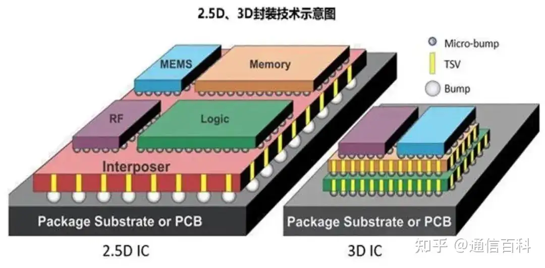
To continuously improve computing power and integration, three more advanced technology paths have been developed: CoWoS, CoPoS, and CoWoP. Today let’s talk about these three types of technology.
█ CoWoS
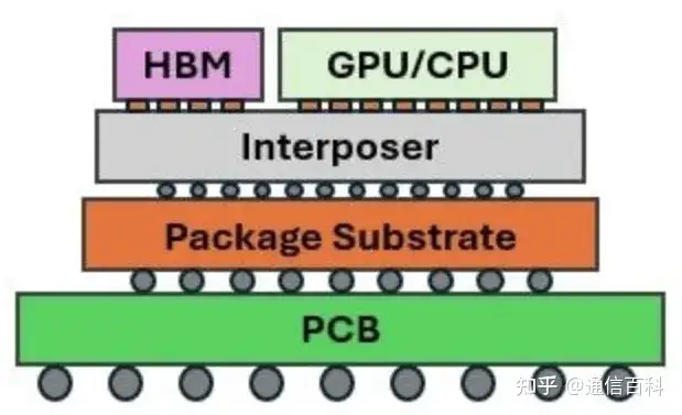
CoWoS (Chip-on-Wafer-on-Substrate): the current mainstream technology, like a “sandwich,” from top to bottom: silicon interposer → ABF substrate → PCB.
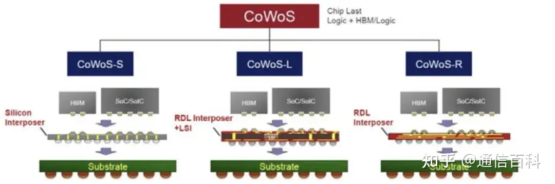
It has evolved into several types according to application needs:
- CoWoS-S: uses a silicon interposer to integrate HBM and GPU, such as NVIDIA H100;
- CoWoS-R: uses a redistribution layer, aimed at cost-sensitive designs;
- CoWoS-L: combines silicon and redistribution layer, supporting a hybrid scheme of up to 12 HBM stacks.

To support this structure, the underlying PCB mainboard must use ultra-low-loss materials (such as Megtron 8) and complex stack-up designs with more than 28 layers, to ensure the integrity of high-speed signal transmission.
█ CoPoS
CoPoS replaces the silicon interposer with a panel-level redistribution layer (usually over 600×600 mm in size), forming a new “RDL → ABF substrate → PCB” structure.
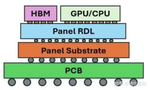
The benefits of this approach are very obvious:
- Panel utilization rises from 85% to over 95%, more economical;
- Cost is reduced by 20-30%;
- It can support the 10-12 HBM4 memory stacks required by future AI servers, providing up to 19 TB/s of bandwidth.
█ CoWoP
CoWoP (Chip-on-Wafer-on-PCB) directly bonds the silicon interposer to the PCB, eliminating the ABF substrate.
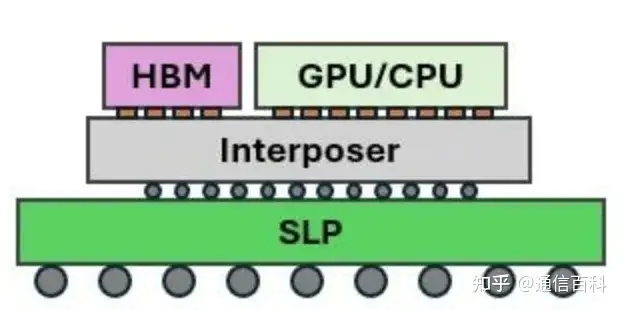
This scheme is said to reduce cost by 40-50%, with a shorter signal path, support for high-speed interfaces such as PCIe 6.0, and improved thermal management efficiency through direct contact with the heat spreader. But its implementation relies on the modified semi-additive process (mSAP), requiring the PCB to achieve line width/spacing ≤25 μm, void-free via filling, and the use of ultra-low coefficient of thermal expansion materials.
█ Comparison
From a technical comparison, the three schemes each have their own advantages.
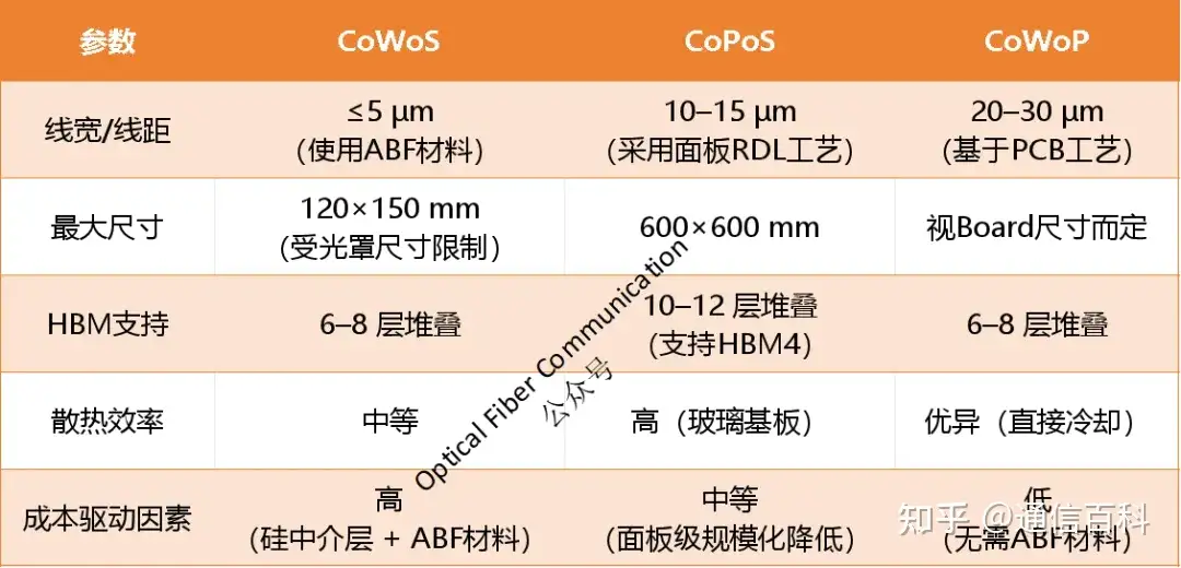
Although CoWoP stands out in terms of cost, it still faces multiple challenges: PCB line width precision (25 μm) lags behind that of the ABF substrate (≤10 μm), the coefficient of thermal expansion mismatch between the chip and PCB materials, and an ecosystem that is not yet mature (currently only Apple’s SLP PCB is close to its requirements).
This also brings opportunities for PCB material innovation: new materials such as low-thermal-expansion glass cloth (such as Nittobo NE-glass), peelable copper foil (such as Fangbang Electronics), and cationic resins, as well as new processes such as mSAP fine-line processing and via filling electroplating (POFV), will become key breakthrough points.
CoPoS technology requires the PCB to be compatible with large panels from 310×310 mm to 700×700 mm, and to support redistribution layer integration through glass via (TGV) substrates.
According to market planning, this technology will establish pilot production lines in 2026-2027 (led by TSMC) and achieve mass production in 2028. The currently mainstream CoWoS technology still requires the PCB industry to focus on solving the impedance control of 56+ Gbps signals (deviation controlled within ±3%), as well as stack-up designs of hybrid FR-4/high-speed materials with more than 40 layers.
For PCB manufacturers, it may be necessary to advance strategic layout in stages:
- Short-term (2025-2026): focus on meeting the 18-46 layer HDI PCB required by CoWoS-L;
- Mid-term (2027-2028): cooperate with packaging and testing factories to develop CoPoS panel-level substrates;
- Long-term (after 2029): deploy CoWoP production lines according to technology maturity, serving edge computing and AI accelerators.
It is worth noting that although CoPoS and CoWoP have significant cost and performance potential, CoWoS is still the mainstream technology supporting current AI chips (such as NVIDIA’s Rubin platform).
Thanks for reading!
Recommended reading:
DIP, SOP, QFP, and LCC Packaging of Chips
ZTE: A Liquid-Cooled Optical Transceiver Structure Supporting CPO
A CPO Packaging Structure Based on Glass Carrier
An Innovative CPO Fiber Vertical Coupling Scheme
SMIC’s Innovative Silicon-Germanium Planarization Process
Enjoy this article?
Subscribe to get new optical communication insights delivered to your inbox. Free, unsubscribe anytime.