The evolution direction of data center optical interconnection is to continuously shorten the copper interconnect traces between chips and optical devices. The further to the next generation, the less copper is used, and the higher the proportion of the optical path.
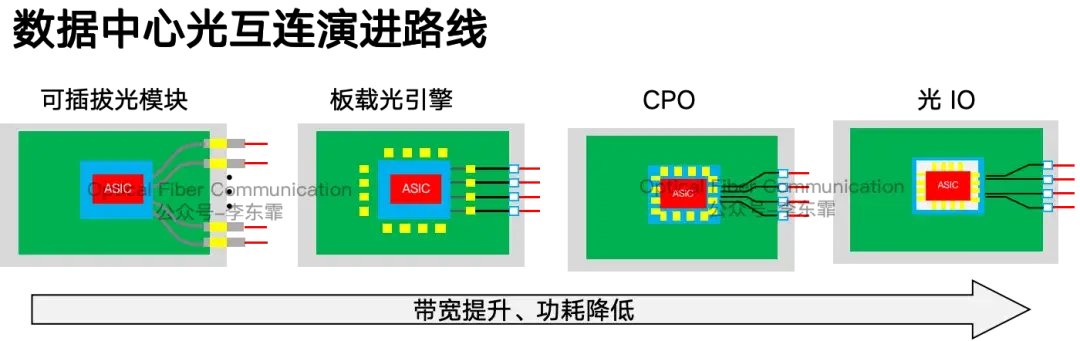
From QSFP pluggable modules, BGA/LGA on-board optical engines, to advanced packaging CPO and on-chip optical IO, packaging has gradually moved toward integration, and the single optical engine rate has also risen from 100G, 400G, 800G all the way to 12.8T and above.
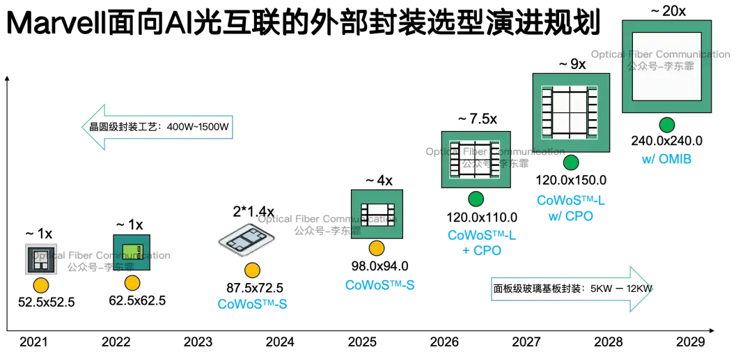
At this year’s OFC 2026, Marvell introduced its technology roadmap for external packaging selection.
Marvell: The Technical Evolution and Product Roadmap of 1.6T Coherent Optics
Marvell: Two New Schemes to Improve the Bandwidth of Silicon-Germanium Detectors
Some Views on Marvell’s Scale Up/Out + the 102.4T CPO Switch
From 2021 to 2022, Marvell mainly used traditional small-size packaging, with areas of 52.5×52.5 and 62.5×62.5 respectively. This kind of packaging can only adapt to QSFP pluggable optical modules, supporting 100G, 400G, and 800G rates.
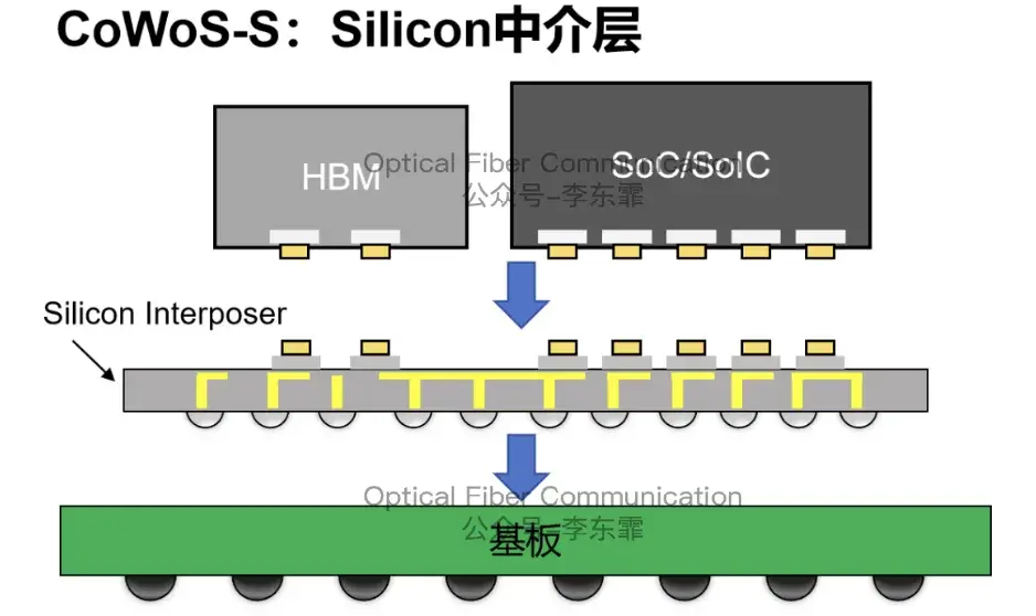
From 2023 to 2025, Marvell chose TSMC’s CoWoS-S silicon interposer packaging, carrying its own CPO photonics architecture, supporting on-board BGA/LGA optical engines, with rates reaching 800G to 1.6T.
From 2025 to 2028, Marvell will adopt CoWoS-L to realize CPO, with the optical engine directly mounted on the surface of the package interposer or substrate.
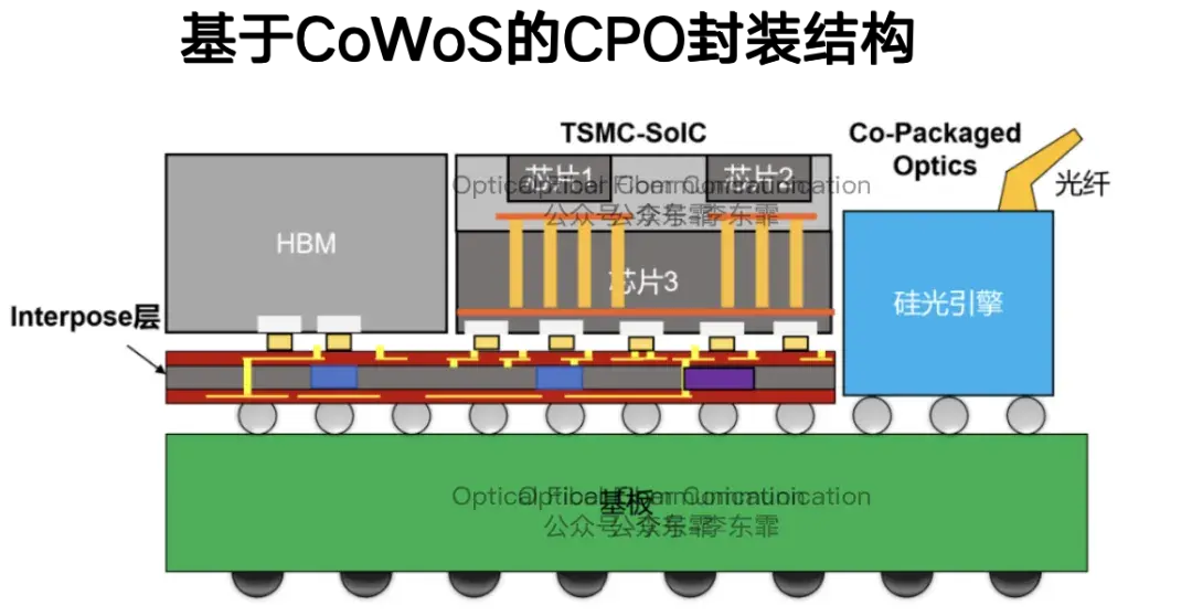
TSMC: CPO Evolution Roadmap Based on COUPE and CoWoS Packaging
The interposer of CoWoS-L contains both LSI (local silicon interconnect) and RDL. Positions requiring high-density interconnection use silicon bridges, while other places use RDL or substrate routing.
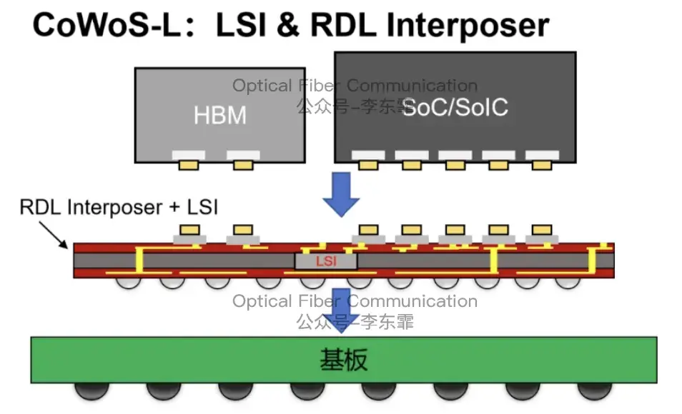
TSMC: CPO Evolution Roadmap Based on COUPE and CoWoS Packaging
TSMC: Silicon Photonics Device Performance and Process Platform for CPO
TSMC: CPO Packaging Flow Based on Silicon Photonics TDV Process
Among them, the XPU, IO die, and CPO three bare dies are laid side by side on the silicon interposer, completing the optical-electrical interconnection through D2D lateral copper interconnect.
But as the package size continues to grow and the pin pitch continues to shrink, a large number of copper D2D interconnects, multi-layer SerDes, and optical-electrical conversion bring additional power consumption.
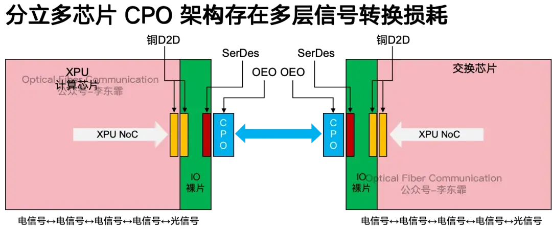
Bandwidth is also limited by trace length and the skin effect. At high frequencies, the skin effect brings obvious RF loss; to increase bandwidth, one can only increase the number of channels or lengthen the copper traces, but this further pushes up power consumption and latency.
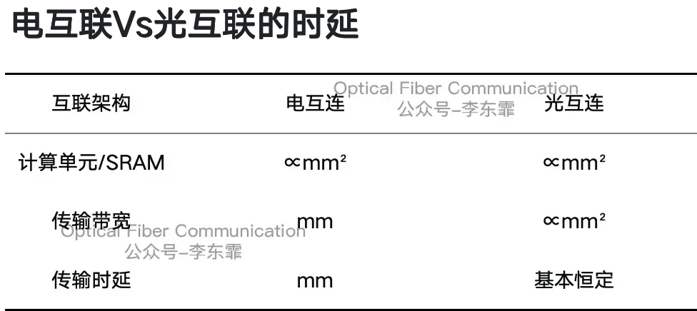
At the same time, the area of computing and memory bare dies continues to expand, and the distance of peripheral I/O copper interconnect is correspondingly lengthened. The transmission delay of copper electrical signals increases linearly with trace length; the longer the trace, the higher the latency.
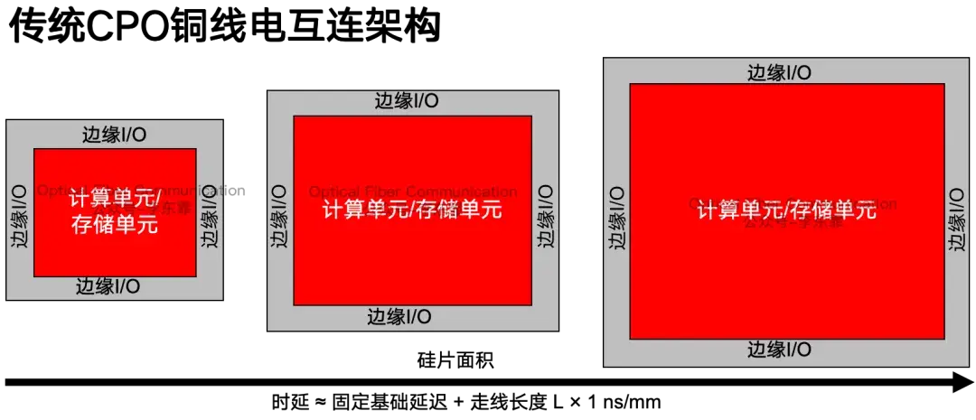
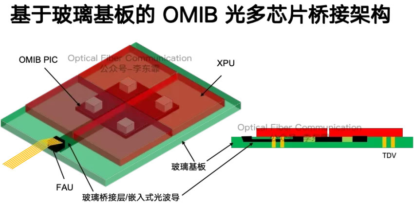
Therefore, in the long-term year 2029, Marvell plans to adopt the OMIB glass substrate packaging obtained after acquiring Celestial AI. The glass substrate embeds optical waveguides, landing the next-generation Optical I/O all-optical interconnection, with the overall package scale expected to reach 20 times that of the first-generation scheme. In our previous article we mentioned Intel’s EMIB electrical silicon bridge scheme.
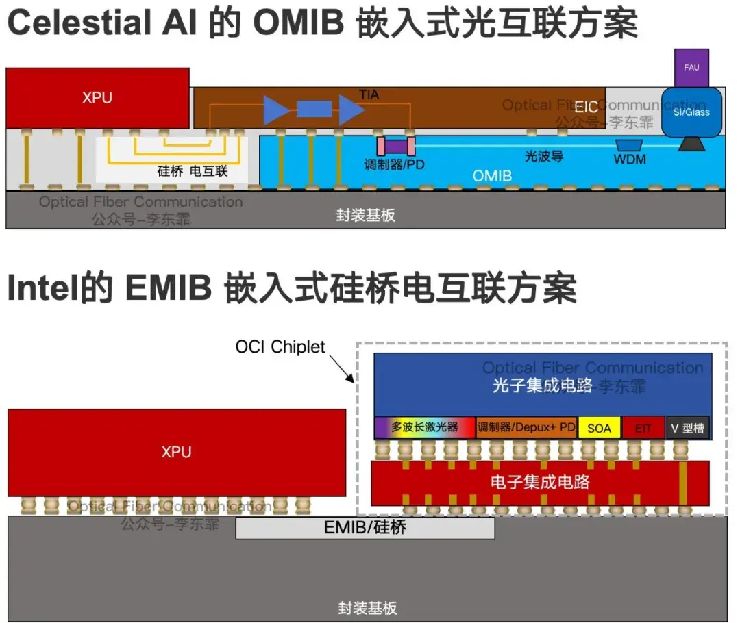
Intel: Progress and Views on the CPO Scheme for OCI
HiSilicon / Intel: SiN-SOI Microring Modulator for CPO
Glass substrate has a low coefficient of thermal expansion and high temperature resistance, supporting 240 mm ultra-large panel-level packaging. The package scale reaches 20 times that of the first generation, and the whole machine can carry ultra-high computing power of 5 kW to 12 kW.
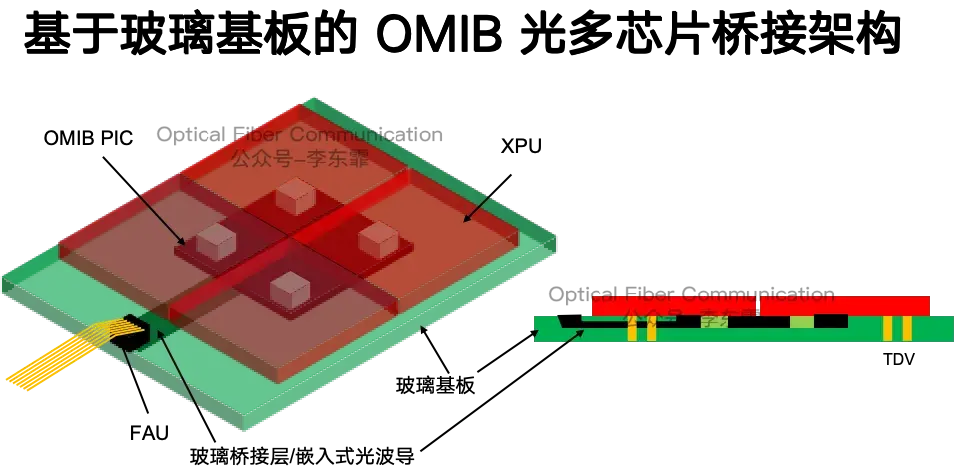
The upper and lower bare dies are mounted on the glass-core substrate, and metal electrical routing and embedded optical waveguides are arranged inside the substrate, realizing high-density interlayer interconnection through TDV vertical vias.
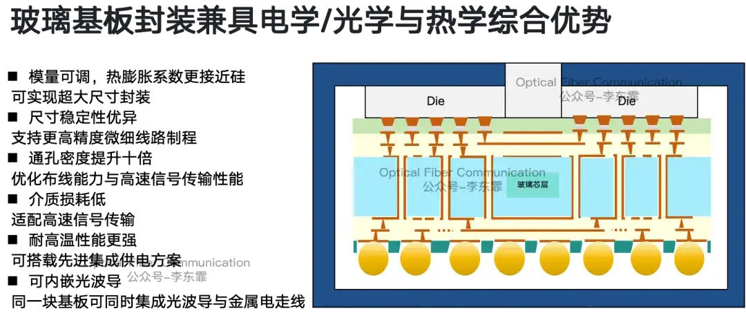
After replacing the vast majority of copper wires with optical channels, the per-unit-distance loss of optical waveguides is far lower than that of copper, fundamentally avoiding the RF loss brought by the high-frequency skin effect.
The latency of OMIB glass substrate Optical I/O optical interconnection barely changes with routing distance.
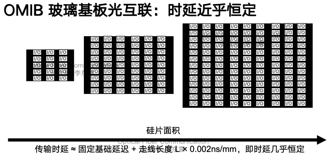
Finally, let’s make a brief comparison.
Welcome to subscribe to our column:
If there are any inaccuracies, please point them out.
Related Reading
- Coherent FY2026 Results (Including CPO Business Panorama)
- Coherent Traveling-Wave Electrode High-Speed EML Scheme
Enjoy this article?
Subscribe to get new optical communication insights delivered to your inbox. Free, unsubscribe anytime.