
The NVIDIA GH200 is probably one of the most easily misunderstood products on the market today. At the same time, after reading related articles, we realize that a basic introduction may still be needed for this highly innovative product launched by NVIDIA.
PS: The term “GH200” may refer to different hardware configurations. Unlike AMD or Intel, which launch multiple models, NVIDIA usually promotes only a single product.
Now let’s clarify the common misconceptions about this chip and briefly talk about its actual use.
The following is the official NVIDIA GH200 diagram:
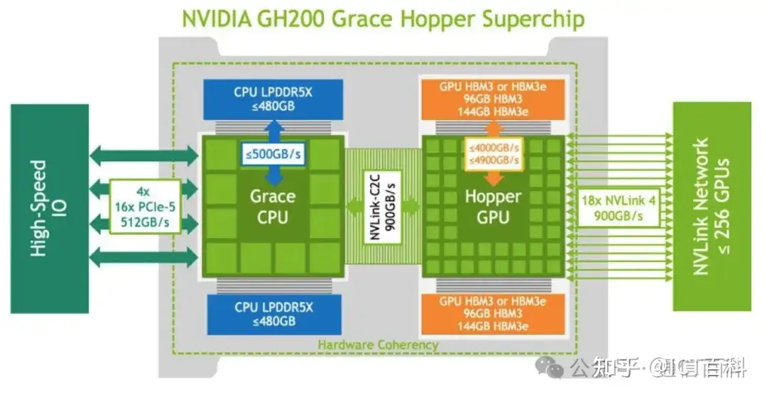
NVIDIA GH200 diagram, September 2024
Regarding NVIDIA’s product, it has two key innovations.
First, LPDDR5X memory is directly soldered onto the chip package. Second, NVLink-C2C provides a high-bandwidth interface between the CPU and GPU.
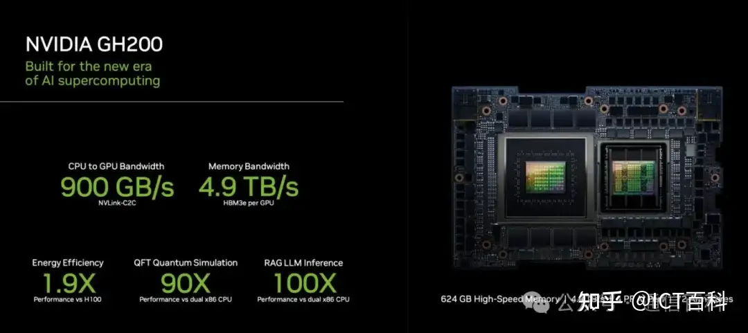
NVIDIA GH200 overview
At the same time, this product uses 72 Arm v9 cores, based on the 2022 Arm Neoverse V2 architecture, not entirely new technology. NVIDIA did not design its own Arm cores like Apple, Qualcomm Oryon, or AmpereOne did.
Speaking of LPDDR5X memory, people often mistakenly think that the GH200 is only equipped with 480GB of memory. However, the actual situation is more complex. Besides the 480GB version, NVIDIA also launched a 120GB bandwidth-optimized version and a 240GB version. According to NVIDIA’s specifications, the 480GB version has a memory bandwidth of 384GB/s, while the 120GB and 240GB versions have a memory bandwidth as high as 512GB/s.
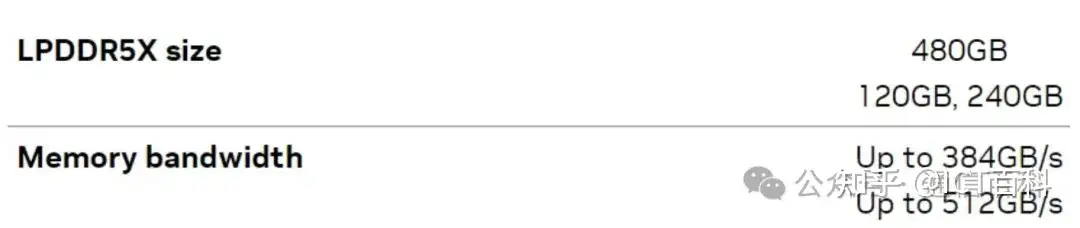
NVIDIA GH200 memory size and bandwidth specifications
A major innovation by NVIDIA is integrating memory directly on the chip package, eliminating the traditional motherboard and DIMM slots, thereby achieving high performance while reducing power consumption. This also means the power consumption of the NVIDIA GH200 includes the consumption of system memory.
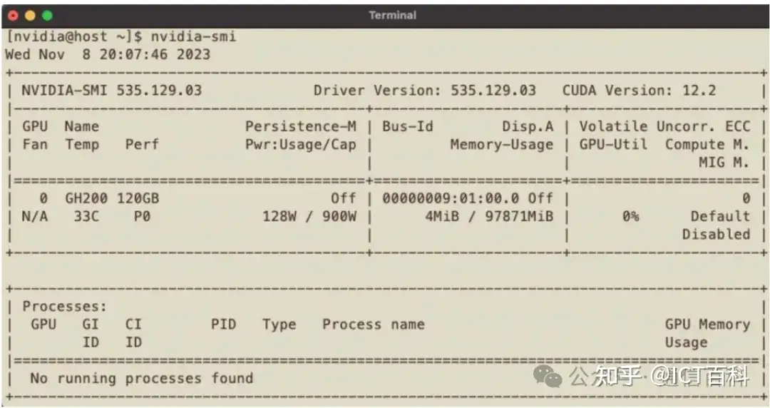
NVIDIA GH200 with 120GB of memory
Shown below are top-view comparison photos of the GH200 and Grace Superchip, each showing the 8 LPDDR5X memory packages equipped on the 72-core Arm CPU.
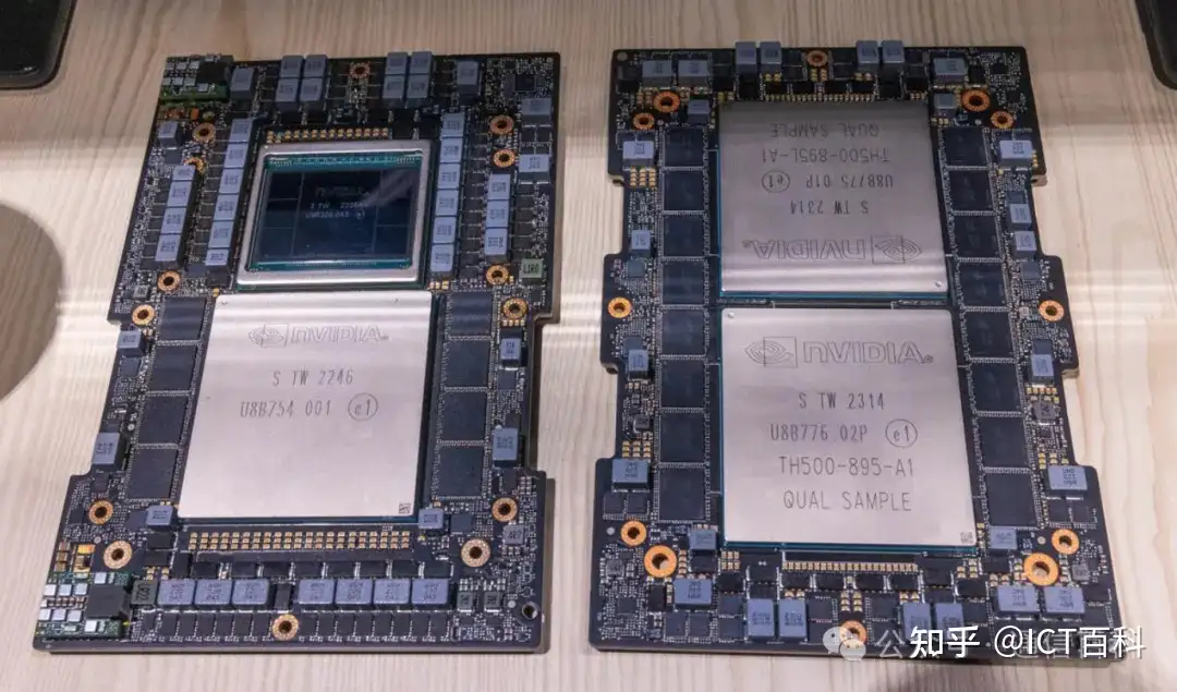
NVIDIA Grace Hopper and NVIDIA Grace superchip
And at the bottom, there are also LPDDR5X packages, so that each CPU has a total of 16 memory packages.
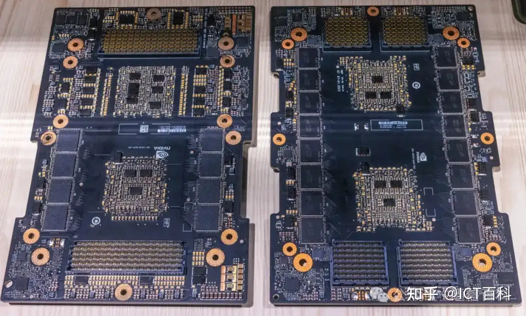
NVIDIA Grace Hopper and NVIDIA Grace superchip
In addition, the Grace CPU side of the GH200 provides 64 PCIe Gen5 lanes, organized into 4 x16 root complexes.
Although this number is far lower than standard server components, since the Hopper GPU is connected via NVLink-C2C rather than PCIe, it cannot be directly compared with AMD EPYC, Intel Xeon, or other CPUs.
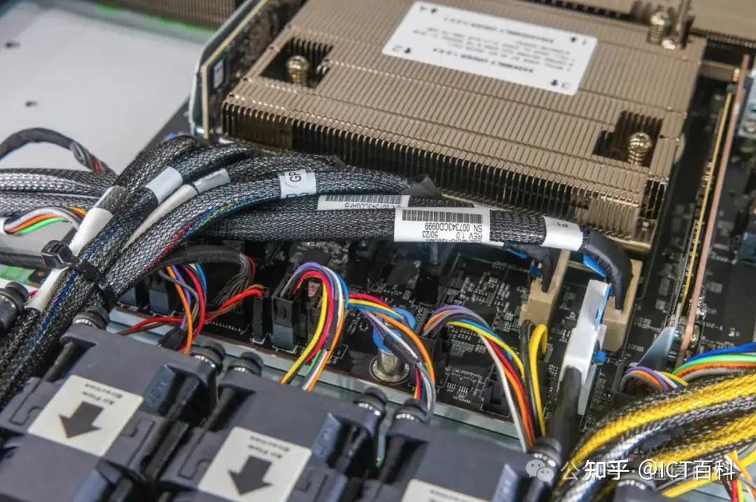
Supermicro ARS 111GL NHR NVIDIA GH200 system MCIO cable
Nevertheless, these lanes are still used to connect InfiniBand or Ethernet adapters / DPUs.
In terms of PCIe connectivity of the GH200 system, if two boot drives are used, 8 of the 64 lanes will be occupied. For the scale-out InfiniBand adapter and the BlueField-3 DPU for the storage network, 16 lanes each, a total of 32 lanes, or half of the 64 lanes, will be occupied.
On the GPU side, although we call it “GH200”, this does not mean the onboard GPU is necessarily the H200 variant. In fact, there are two versions: 96GB and 144GB.
The standard NVIDIA H100 comes with 80GB of PCIe HBM2e, while the SXM5 GPU comes with 80GB of HBM3. Even the H100 memory configuration differs, but this point is often overlooked. The 80GB memory on the standard H100 is distributed across five stacks, each 16GB.
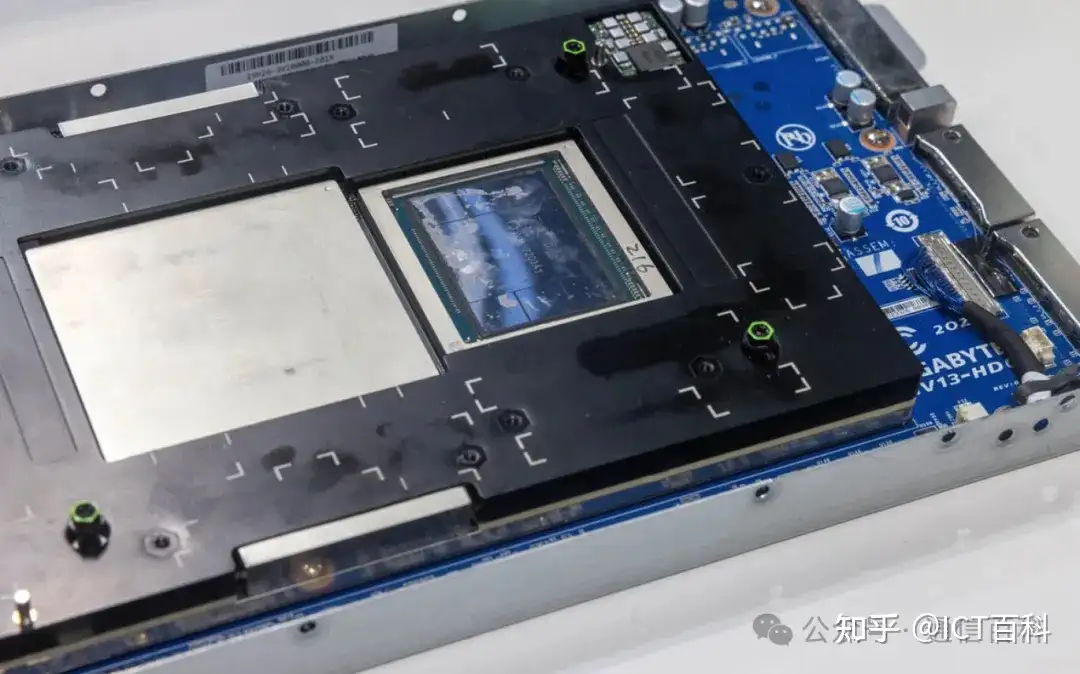
Gigabyte H223 V10 2U4N NVIDIA Grace Hopper node GH100
The 96GB version includes all six stacks visible around the package. Due to memory retention for yield reasons, we may also see a 94GB version. This is similar to the case of the 141GB variant of the H200 equipped with 144GB.
Therefore, when we mention the NVIDIA H100, it can have an 80GB or 96GB memory configuration, and can be HBM2e or HBM3. And when we mention the NVIDIA H200, we are referring to the 144GB (141GB) HBM3e version. When we say GH200, the Hopper side can be a 96GB H100 HBM3 GPU or a 144GB (141GB) HBM3e H200 GPU.
So our previous statement is correct: the GH200 is an updated version of the GH100. Although both use the “GH200” name, it is also possible to get an H100 GPU in the GH200.
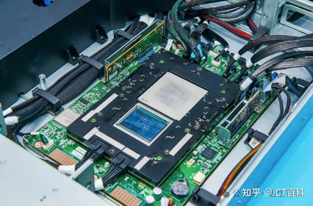
QCT QuantaGrid S74G 2U with NVIDIA Grace Hopper installed
At this point, everyone may realize that with three LPDDR5X memory configurations and two HBM configurations, a single “GH200” name indeed covers a lot of content.
Besides these, there is still another dimension to consider: power.
The operating power range of the NVIDIA GH200 is from 450W to 1000W. Most devices running at the 1kW level will use liquid cooling. 450W is extremely low for a CPU, GPU, and memory. NVIDIA only needs to use the “nvidia-smi –power-limit=” tool to sell its GPUs with a range of configurable TDPs. Average frequency does not scale linearly with voltage, but if there are 500W TDP and 1000W TDP, the performance difference will be significant.
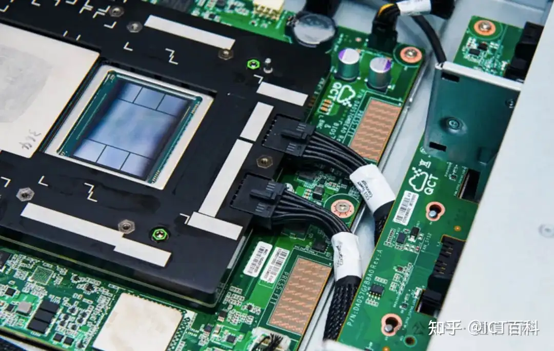
QCT QuantaGrid S74 2U NVIDIA Grace Hopper power
For those who do not know this, another interesting part of the GH200 is that power comes directly from the power supply plugged into the GH200 package. Whereas in a typical server, the CPU gets power from the motherboard.
Finally, to review, when someone mentions the GH200, besides the facts that it has Arm Neoverse V2 cores and an NVIDIA Hopper GPU, there are still some huge differences in its meaning. We can have:
- 120GB, 240GB, or 480GB LPDDR5X memory for the CPU;
- 384GB/s or 512GB/s LPDDR5X memory bandwidth for the CPU;
- 96GB HBM3 or 144GB (141GB) HBM3E for the GPU;
- 4TB/s (HBM3) or 4.9TB/s (HBM3E) GPU memory bandwidth;
- A large performance range, depending on the TDP setting.
These diverse configurations are all called “GH200”, which is, so to speak, an extremely broad range.
Overall, since the GPU in the GH200 may be more like an SXM5 H100 or H200, and the TDP may be very different, when we discuss the NVIDIA Grace Hopper, it is very important to clarify its version.

Enjoy this article?
Subscribe to get new optical communication insights delivered to your inbox. Free, unsubscribe anytime.