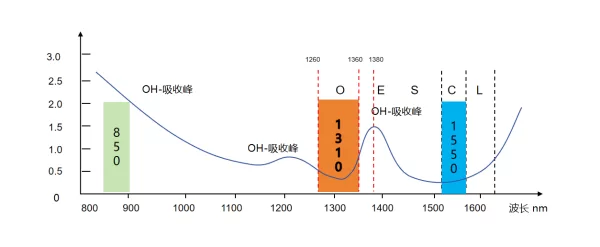
When electromagnetic waves propagate in different media, their characteristics are often highly selective. This is particularly evident in silica optical fiber. Although the electromagnetic spectrum is extremely broad, including various radiations from microwaves to gamma rays, the optical band in which optical fiber communication can actually work effectively is limited to a very narrow range in the near-infrared region.
As shown in the figure below, this specific low-loss region is the “transmission window” of optical fiber communication.
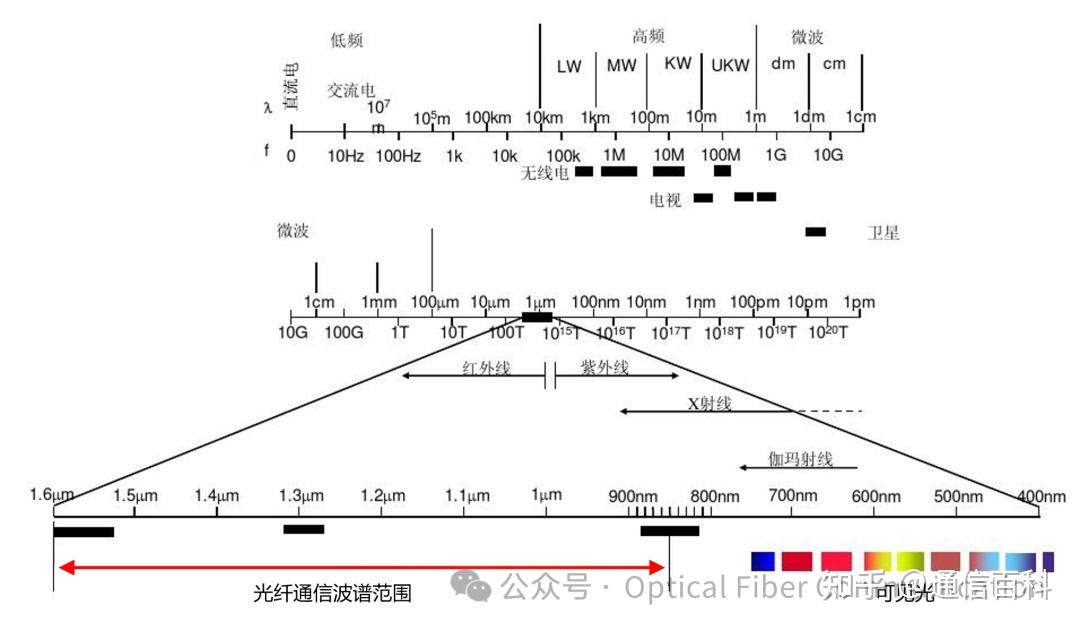
The spectral range where the red arrow is located is mainly determined by the intrinsic absorption characteristics of silica material (ultraviolet electronic absorption, infrared vibrational absorption) and Rayleigh scattering loss.
Understanding the loss mechanism requires clarifying the relationship between photon energy (E) and its wavelength (λ). As an energy quantum, the energy of a photon is proportional to the frequency (ν) of the electromagnetic wave.
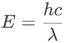
- E: photon energy (unit: joule J or electron volt eV);
- h: Planck’s constant;
- c: speed of light in vacuum (3×10⁸ m/s);
- λ: photon wavelength (unit: m).
Physical essence: as an energy quantum, the energy of a photon is proportional to the frequency ν of the electromagnetic wave (E=hν). Since wavelength and frequency satisfy c=λν, energy is inversely proportional to wavelength.
The attenuation mechanism of silica glass (the core material of optical fiber) to light mainly originates from three types of physical effects:
1. Electronic absorption: when the photon energy > 9 eV (wavelength < 138 nm), photons can excite valence band electrons to transition to the conduction band, causing strong light absorption. For example, near a wavelength of 200 nm, the loss can be as high as several thousand dB/km or more. Since the operating wavelength of optical fiber communication is far greater than this, the impact of this mechanism is negligible.
2. Molecular vibrational absorption: occurs when the photon energy matches the vibrational energy level of the molecular bond. For example, at 1383 nm, the OH bond resonates strongly (like a particularly high speed bump), causing a strong hydroxyl absorption peak.
3. Also, above 1600 nm, the Si-O bond vibration consumes energy (like a continuous group of speed bumps on the highway), causing multiphonon absorption.
How to understand the three points above in plain terms? Let’s imagine the optical fiber as a highway, and light as the trucks running on it.
Level 1: Ultra-High Wall (Deep Ultraviolet Absorption)
- Checkpoint position: before 138 nanometers (10 times shorter than violet light);
- Checkpoint principle: a 9-meter-high brick wall (corresponding to 9 eV energy);
- Truck encounter: only supercars (deep ultraviolet light) can crash through the wall, but the car and passengers will be destroyed (light energy is completely absorbed);
- Real impact: the light of daily communication never reaches here, so it can be completely ignored.
Level 2: Continuous Speed Bumps (Infrared Vibrational Absorption)
- Checkpoint position: after 1600 nanometers (twice the wavelength of red light);
- Checkpoint principle: dense rubber speed bumps (corresponding to molecular bond vibration);
- Truck encounter:
- At 1383 nanometers: there is a particularly high speed bump (hydroxyl absorption peak);
- >1600 nanometers: increasingly dense speed bumps (multiphonon absorption);
- Real countermeasure: either detour around it or eliminate it.
Level 3: Random Dense Fog (Scattering Loss)
- Fog position: the entire highway, but denser in the short-wave region;
- Fog principle:
- 400-1600 nm segment: light fog (Rayleigh scattering), densest in the blue region (∝ 1/λ⁴);
- Defect sections: local sandstorms (Mie scattering, rare in modern fiber);
- Truck encounter: light deviates from the lane like a truck, and energy is gradually lost.
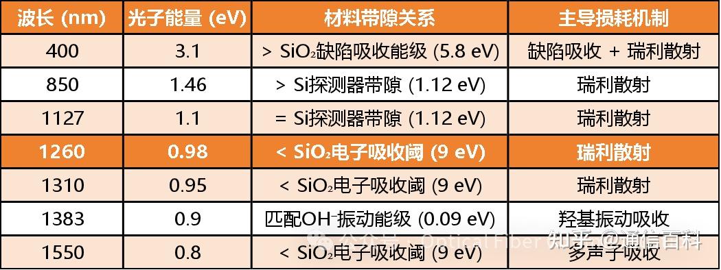
Combining the key data mentioned above, we organize them into the following table:
It should be emphasized that the optical fiber communication system is a whole. The selection of the transmission window depends not only on the loss characteristics of the fiber itself, but must also match the emission wavelength of the light source and the response wavelength range of the detector.
Therefore, in the table above I added two nodes, 850 nm and 1127 nm, mainly based on the matching consideration of light source/detector.
Thus we have the following classic illustration:
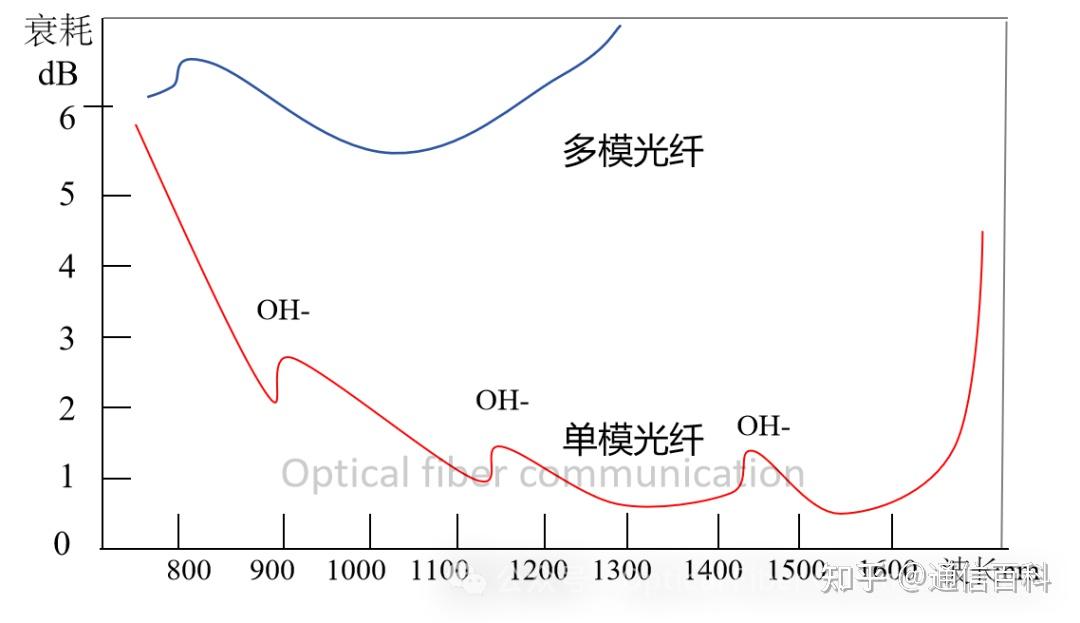
In the early 1970s, with the breakthrough in optical fiber material purification technology (especially reducing the hydroxyl content), the loss of optical fiber in the short-wavelength band (800-900 nm) dropped below 20 dB/km for the first time. This band was established as the “first window” because it was the first to achieve practical use, mainly applied to multimode fiber systems.
At that time, the most mature and economical light source was the gallium arsenide (GaAs) light-emitting diode (LED). As a direct bandgap semiconductor, GaAs has a room-temperature bandgap energy of about 1.42-1.43 eV. According to the approximate relationship between the semiconductor bandgap and the emission wavelength, its cutoff wavelength formula is:
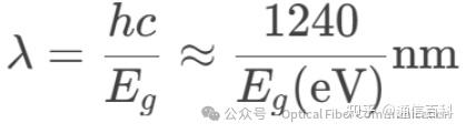
Substituting Eg=1.43eV, we calculate λ≈867 nm, close to the 850 nm band. However, the 850 nm light here is not even laser light, just ordinary LED light.
I have seen some articles saying that the first window of optical communication was designed to match the LED, and I do not fully agree. In my personal view:
Layer 1 is the physical limit: the bandgap of GaAs material determines that the LED can only emit light near 850 nm, which is a natural law. As the only commercially available visible/near-infrared LED material (1970s), GaAs, with its intrinsic bandgap (1.42 eV), forcibly constrains the emission wavelength to near 850 nm through quantum mechanics (calculation: λ=1240/1.42≈870 nm). This is a natural law that humans cannot change.
Layer 2 is material engineering: early silica fiber at 850 nm, although not the lowest loss (0.4 dB/km), was 10 times lower than the 650 nm red light loss, which was the only feasible scheme. If 1300 nm (theoretically lower loss) were used, there was no commercial infrared LED at the time, and the cost of InGaAs detectors was 10 times that of Si PD detectors.
Layer 3 is system compromise: the large-core multimode fiber was essentially a sacrifice made to match the emission area and divergence angle of the LED, otherwise the optical power could not be coupled at all.
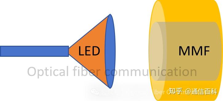
The LED has a large emission area and a wide divergence angle, so it needs to match a multimode fiber with a large core diameter (corresponding to a large mode field diameter MFD) to effectively collect and transmit the optical power it emits.
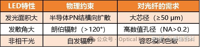
Overall, it can be expressed with the following logic diagram:
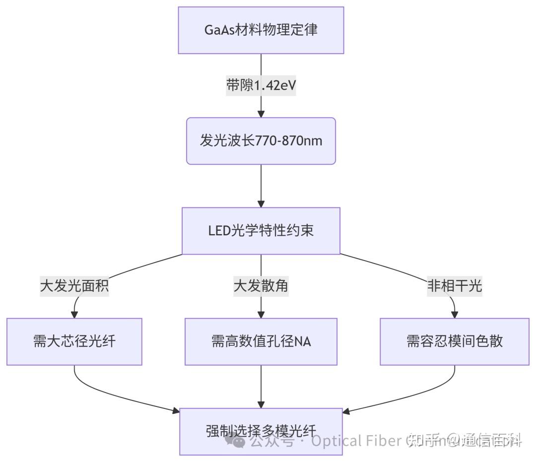
The plain-language explanations of some terms in this diagram, such as numerical aperture and intermodal dispersion, will be written specifically in subsequent articles.
Even today, when lasers dominate, 850 nm + multimode fiber is still the core short-distance scheme, because it inherits two genes from the LED era:
- VCSEL laser: continues the GaAs material system, still most efficient at 850 nm;
- Cost structure: the cost of multimode fiber systems is 1/4 that of single-mode (2023 LightCounting data).
Let’s continue with 1127 nm and 1260 nm. Some may ask, why does 1260 nm suddenly appear?
First, let’s explain where 1127 nm comes from. This requires mentioning the bandgap of the silicon (Si) photodetector (not the bandgap of the fiber SiO2). The bandgap energy of silicon at room temperature is 1.12 eV, which is the theoretical cutoff point of silicon intrinsic absorption. Again using the cutoff wavelength formula above:
λc≈1107 nm
Note: in engineering, the approximate value Eg≈1.1 eV is often taken, at which point λc≈1127 nm. This value can be understood as the security gate of the silicon chip factory (detector characteristic), but it is unrelated to the fiber highway.
Although the engineering cutoff wavelength of silicon is 1127 nm, the Urbach tail causes serious problems in the 1127-1260 nm range. This means that for photons with wavelengths greater than 1127 nm, their energy is insufficient to excite electrons in silicon across the bandgap, and the detector responsivity should theoretically drop to zero.
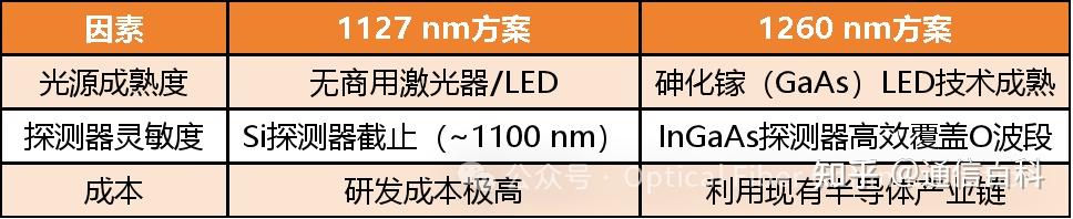
As we mentioned earlier, the transmission window of optical fiber communication needs to consider both the fiber loss and the performance of the light source/photodetector. Therefore, in order to avoid the electronic absorption tail of the detector on the short-wave side, the engineering community moved the starting point of the communication O-band window from the theoretical minimum of 1127 nm to 1260 nm.
Finally, I summarize this section with a table:
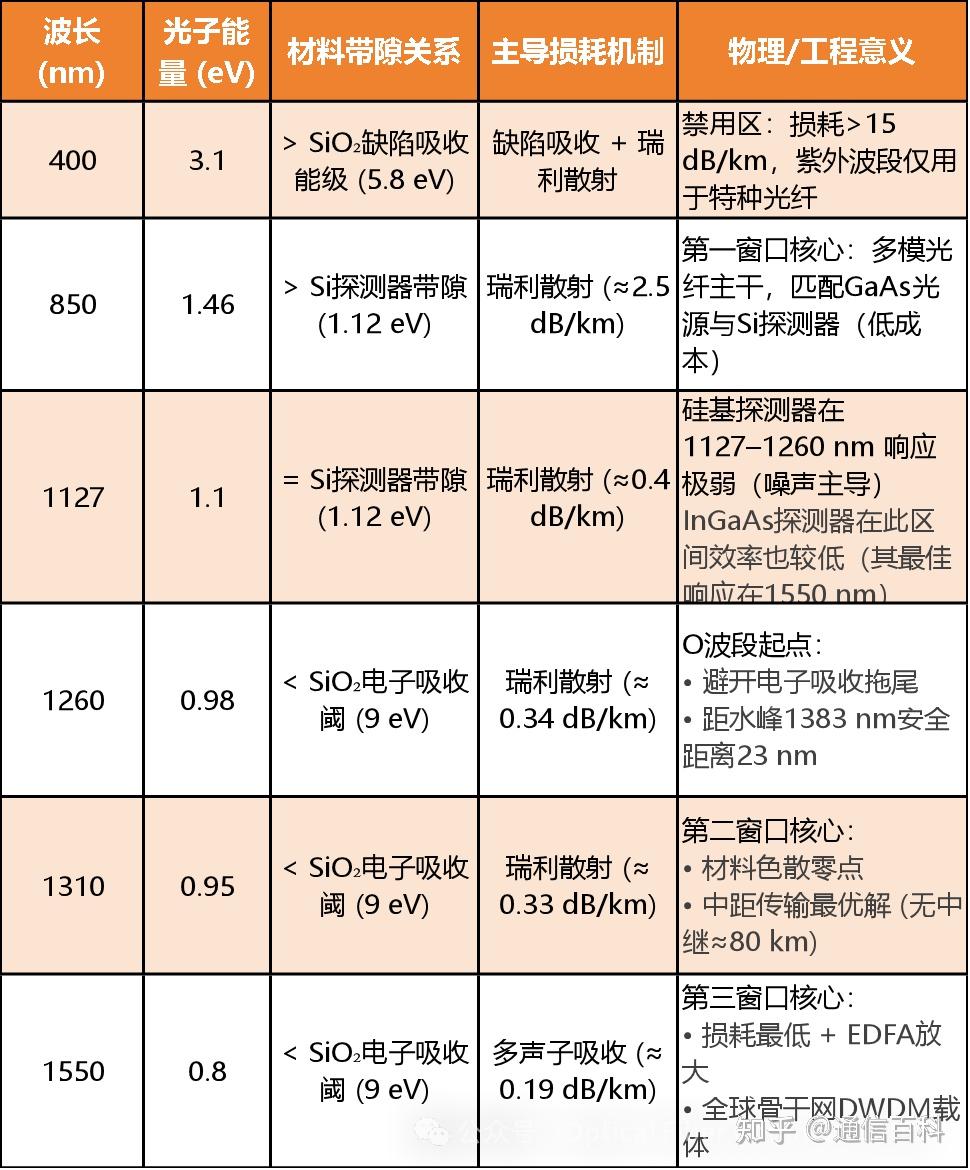
Based on the above content, we have the first window of 850 nm (used by multimode fiber), the second window of 1310 nm (used by single-mode fiber), and the third window of 1550 nm (used by single-mode fiber). These three are the most traditional and most commonly used windows.
Among them, ITU-T further divides the optical fiber communication bands into six bands, O, E, S, C, L, and U, covering a wider range. The O-band is 1260-1360 nm, corresponding to the second window; the C-band is 1530-1565 nm, corresponding to the third window; the L-band is 1565-1625 nm, called the fourth window; and the E-band is 1360-1460 nm, called the fifth window.
Enjoy this article?
Subscribe to get new optical communication insights delivered to your inbox. Free, unsubscribe anytime.