If you are interested in semiconductors / chips / optical device modules / optical fiber communication, etc.
Welcome to follow us!
As Moore’s Law gradually slows down, cramming all functions into one single large chip is not only becoming increasingly difficult technically, but also increasingly expensive. This forces the entire industry to look for new ways out, and the most important direction at present is “heterogeneous integration.”
What is heterogeneous integration?
Simply put, instead of forcing a single large chip, we change the approach and use advanced packaging technology to integrate different functional modules such as CPU, GPU, and memory into the same package, like assembling LEGO blocks.
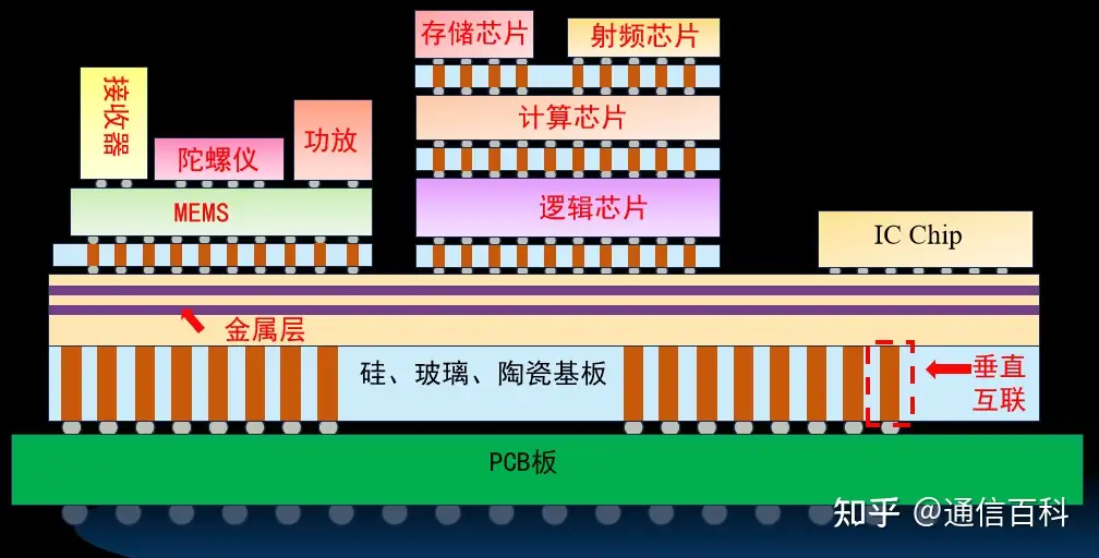
Heterogeneous system-level hybrid packaging process
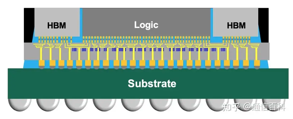
At present, TSMC’s CoWoS, Intel’s Foveros, and Samsung’s X-Cube constitute the three mainstream advanced packaging solutions.
TSMC’s CoWoS:
Intel’s Foveros:
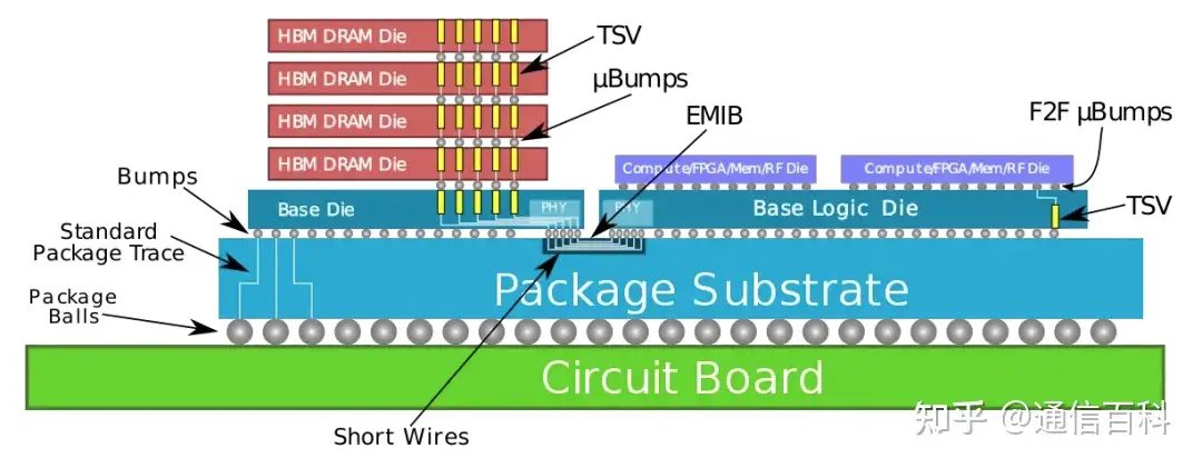
Samsung’s X-Cube:
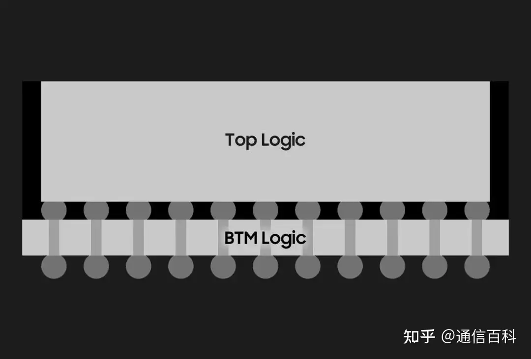
But their specific approaches are somewhat different. Below, we elaborate from the aspects of packaging architecture integration method, interconnect density and performance, design complexity and flexibility, as well as commercial application and deployment.
From the perspective of packaging architecture integration method:
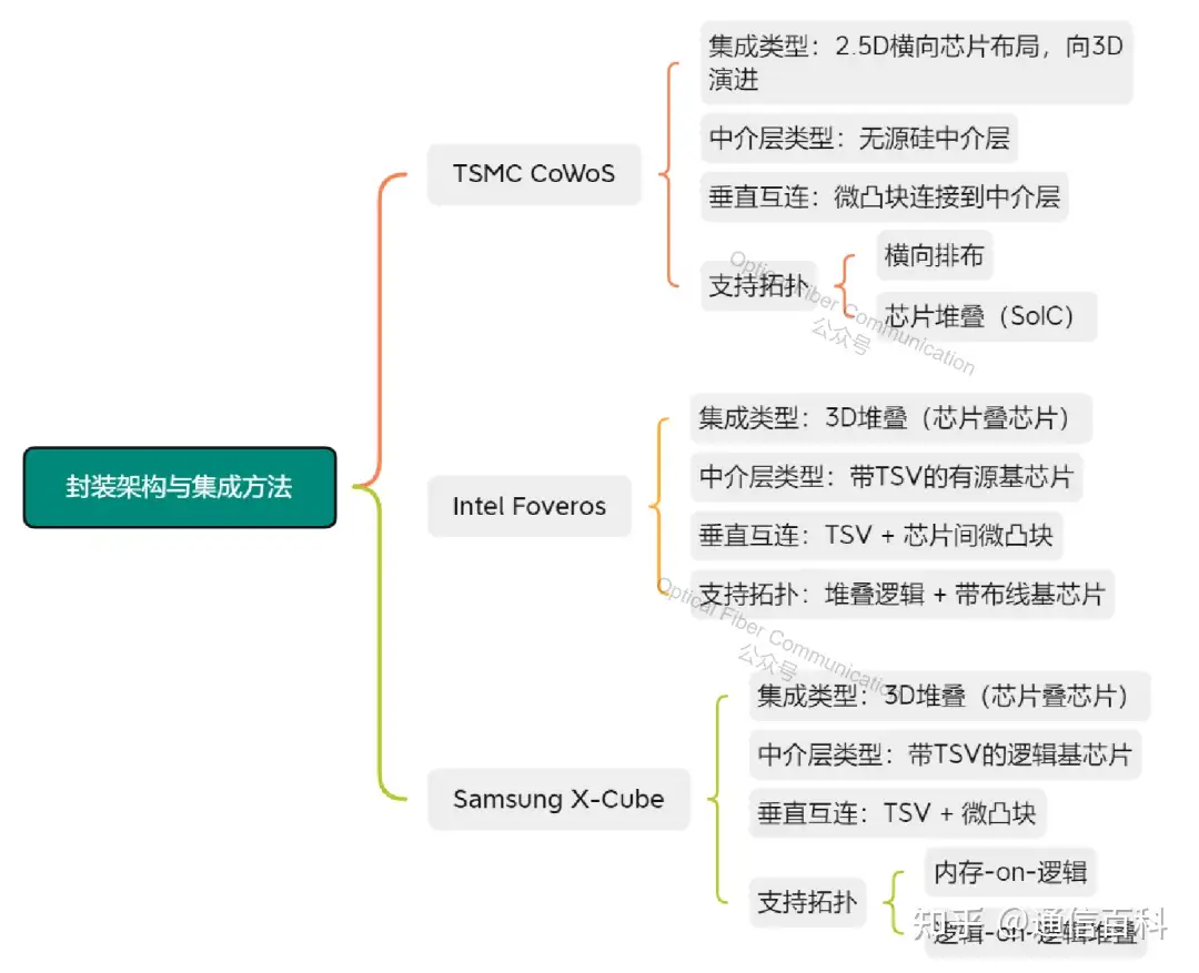
- TSMC CoWoS:
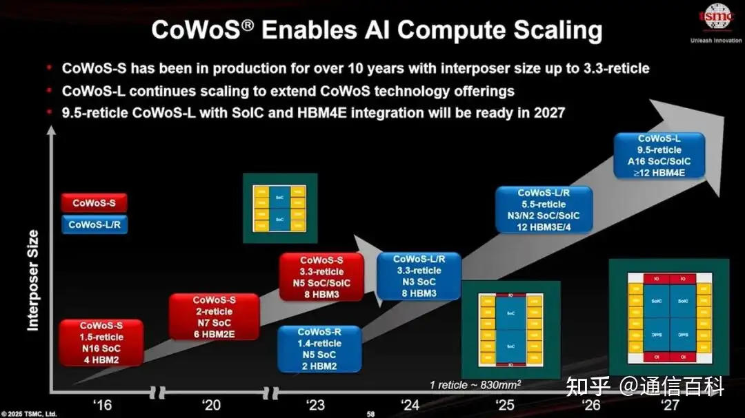
It adopts the “chip-wafer-substrate” architecture to achieve extremely high bandwidth and signal density between chips. It has excellent scalability, supports reticle-size interposers (such as CoWoS-S), and works in coordination with TSMC’s 3D stacking solution SoIC.
- Intel Foveros:
The industry’s first mass-produced logic-on-logic 3D stacking technology, which relies on TSV and fine-pitch micro-bumps for interconnection, supports modular integration across multiple process nodes, and has been used in Meteor Lake client CPUs and subsequent AI accelerators.
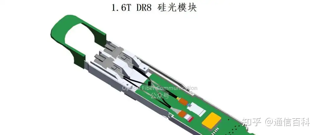
Intel’s 1.6T / 3.2T Optical Module Path
- Samsung X-Cube:
It adopts extremely fine TSV pitch and tight micro-bump spacing, improving thermal control and signal integrity through TSV optimization and co-design, and is currently in the prototype and R&D stage, not yet commercialized at scale.
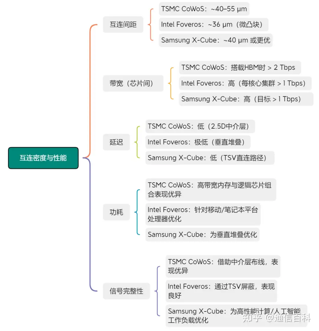
The comparison in terms of interconnect density and performance is as follows:
Thermal management is a key consideration in advanced packaging, and the characteristics of each solution are as follows:
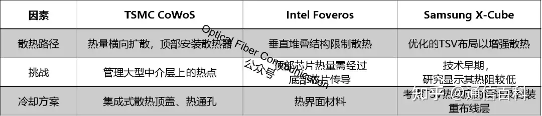
Since stacking logic chips significantly increases power density, Foveros technology faces more severe thermal constraint challenges. CoWoS benefits from the lateral arrangement of chips and heat spreading, giving it more ample thermal management space. X-Cube attempts to improve vertical thermal conductivity by optimizing the layout of TSVs.
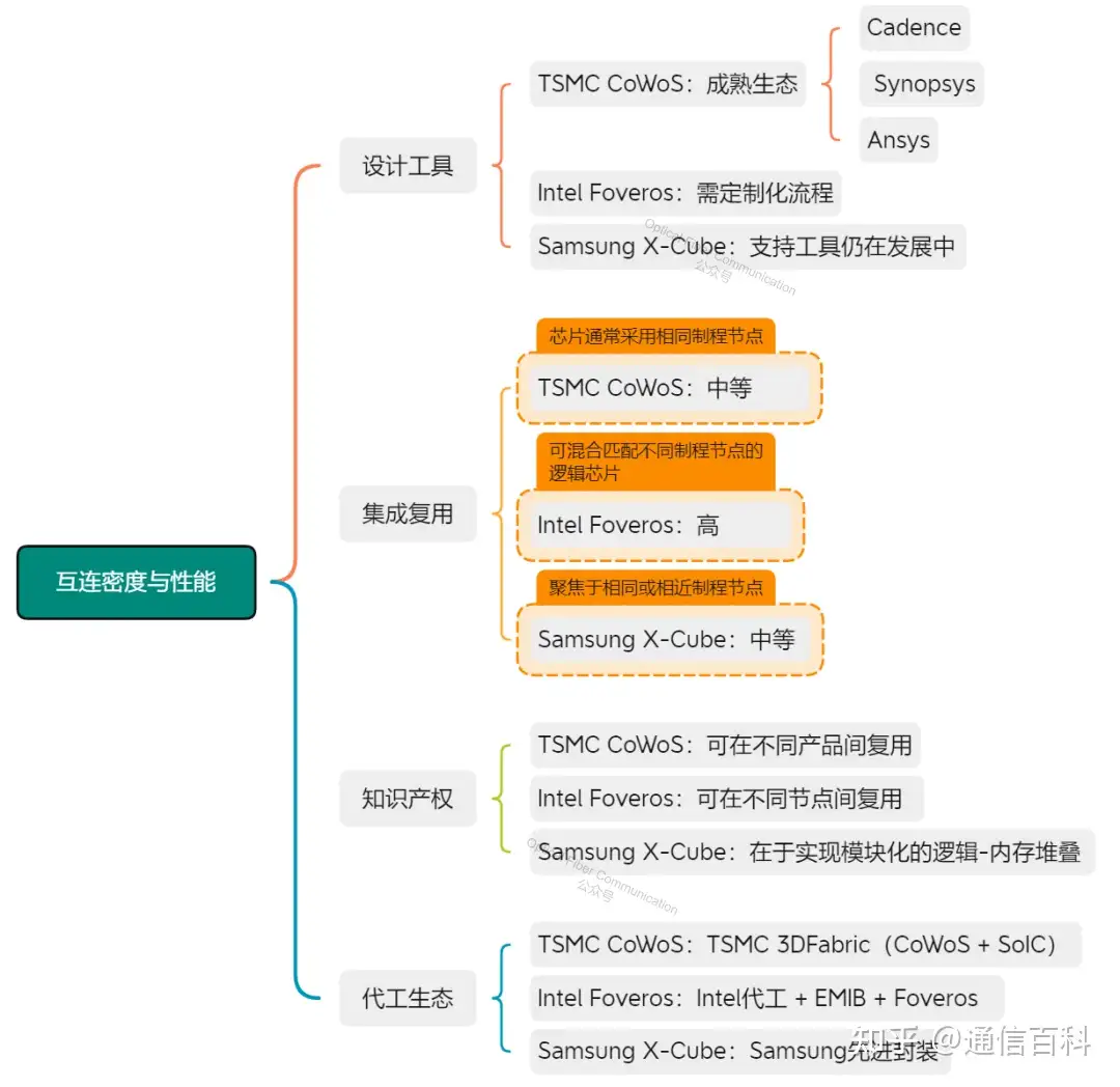
In terms of design complexity and flexibility, the platforms differ:
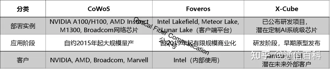
The commercial application and deployment status is as follows:
From a strategic perspective:
- TSMC CoWoS dominates the high-performance computing and artificial intelligence markets, is a key driver of NVIDIA maintaining its GPU leadership, and forms the foundation of TSMC’s 3DFabric platform.
- Intel Foveros is crucial to Intel’s modular design strategy, with its applications expanding from client to data centers and AI accelerators, and will combine with embedded multi-die interconnect bridge technology in the future.
- Samsung X-Cube is Samsung’s focus for competing for packaging technology leadership, closely coordinated with its high-bandwidth memory business, and oriented toward logic-memory co-packaging in future high-performance computing and mobile designs.
The summary comparison table is as follows:
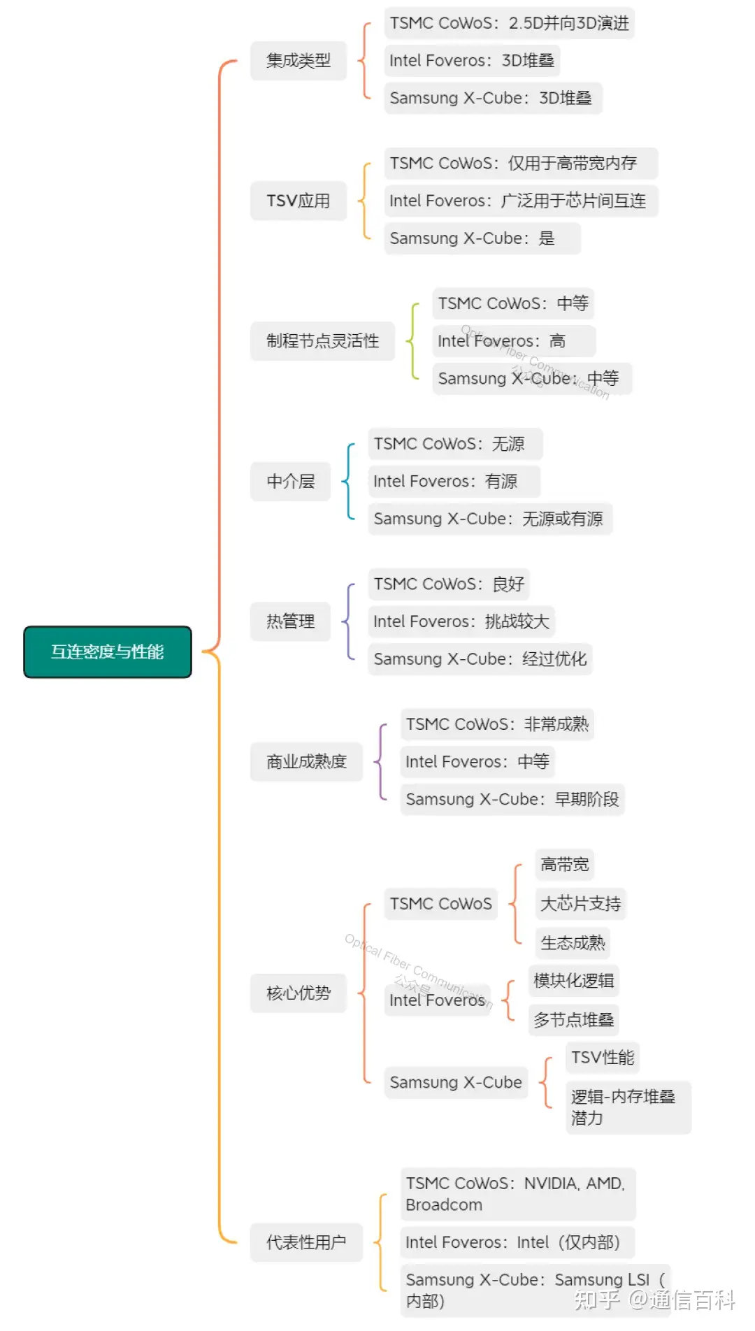
Finally, let us look at the technology development timelines of the three companies:
- TSMC – CoWoS series
- 2011: Launched CoWoS (Chip on Wafer on Substrate) technology;
- 2012: Mass-produced the first CoWoS-based chip, a Xilinx FPGA;
- 2015: CoWoS technology applied to NVIDIA Pascal architecture products;
- 2017: Released the upgraded version CoWoS-S;
- 2020: Launched SoIC technology as a 3D packaging complement to CoWoS;
- 2022: Released the CoWoS-R version;
- 2024-25: Planned to launch CoWoS-3D and SoIC-Direct technologies.
- Intel – Foveros series
- 2018: Publicly announced Foveros 3D stacking packaging technology;
- 2019: Mass-produced the Lakefield processor, the first product based on Foveros technology;
- 2022: Previewed the Meteor Lake processor using Foveros technology;
- 2024: Officially released the Meteor Lake processor;
- 2025: Planned to launch two products based on Foveros technology, Lunar Lake and Falcon Shores.
- Samsung – X-Cube series
- 2019: Started internal development of X-Cube 3D packaging technology;
- 2020: Publicly announced X-Cube technology;
- 2021: Launched an EUV demonstration chip based on X-Cube;
- 2023: Conducted HBM3 memory stacking pilot project (based on X-Cube technology);
- 2025: Goal of achieving logic-memory stacking in AI / HPC (based on X-Cube technology).
Thank you for reading!
Broadcom & HiSilicon: VCSEL NPO/CPO and Silicon Photonics CPO
Related Reading
- Several Advanced Packaging Technologies
- What Is Advanced Packaging?
- CPO and 2.5D/3D Advanced Packaging
Enjoy this article?
Subscribe to get new optical communication insights delivered to your inbox. Free, unsubscribe anytime.