If you are interested in semiconductors / chips / optical device modules / optical fiber communication, welcome to follow us!
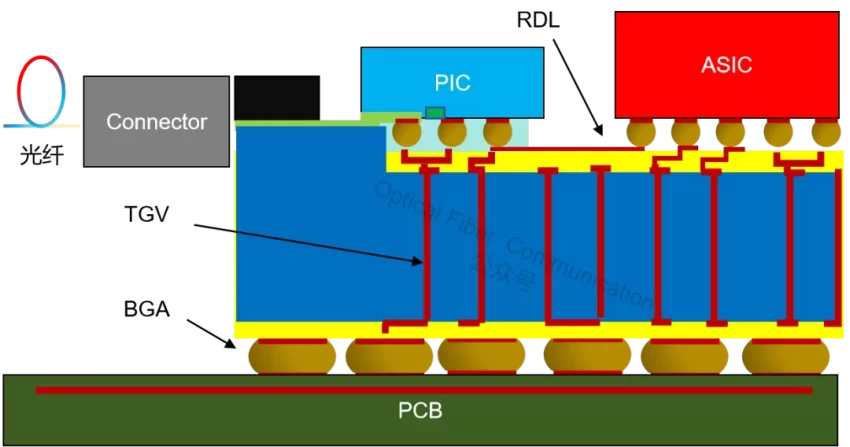
The industry has developed a variety of advanced packaging technologies, such as FO (fan-out), 2D, 2.5D, and 3D integration. These technologies all make use of several key processes, including RDL, silicon- or glass-based interposers, TSV (through-silicon via) and TGV (through-glass via), and so on.
Let us first talk about FO fan-out packaging. Its characteristic is to “fan out” the I/O interfaces of the chip from a small area to the entire large area of the package, forming an external array of solder balls.
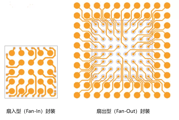
The most direct benefit of doing this is that, while keeping the package size compact, it can provide far more I/O than traditional packaging.
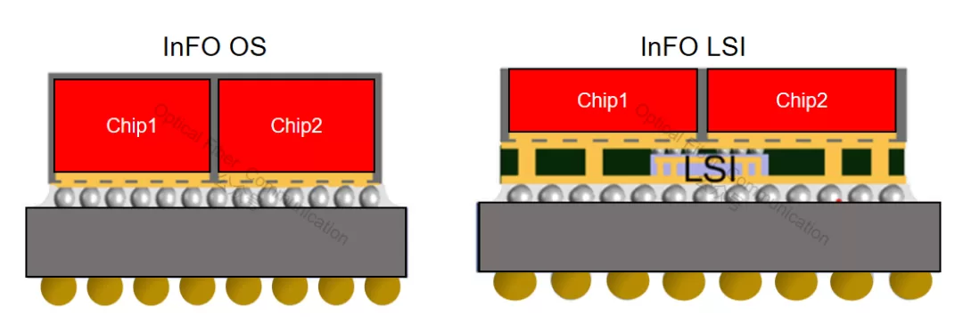
In this field, TSMC’s InFO (Integrated Fan-Out) technology is a typical representative. It has spawned several variants, such as InFO PoP, InFO B, InFO OS, and InFO LSI.
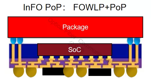
Among them, InFO PoP is a 3D package that combines FOWLP (Fan-Out Wafer-Level Packaging) technology with PoP (Package-on-Package) design.
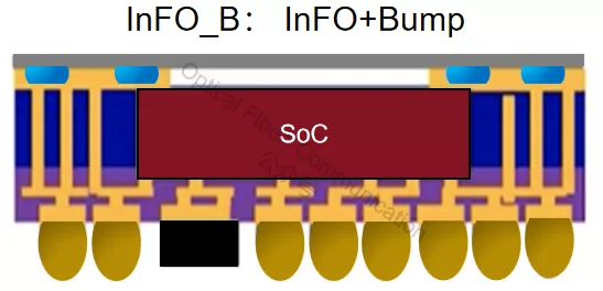
InFO B, that is InFO Bump, mainly integrates bumping technology into the fan-out structure. Its main difference from traditional InFO is the addition of bumps on the substrate.
We will not elaborate on InFO OS (InFO Open Substrate) and InFO LSI (InFO Logic System Integration); their structural schematics are as follows:
Now let us talk about 2D advanced packaging. As the name implies, it arranges multiple chips or dies on the same substrate in a planar manner.
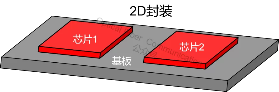
The chips are connected through fine-pitch interconnect technologies, such as wire bonding, flip-chip, or advanced bonding techniques like micro-bumps.
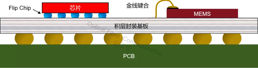
Further reading: From C4, Cu Pillar to Cu mu-Pillar!
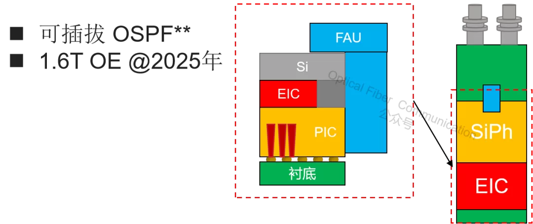
Based on 2D advanced packaging technology, TSMC designed a COUPE 2D CPO solution in 2021. The COUPE platform uses a 65nm process on 12-inch wafers. In this solution, the EIC and PIC are integrated together through a bonding process.
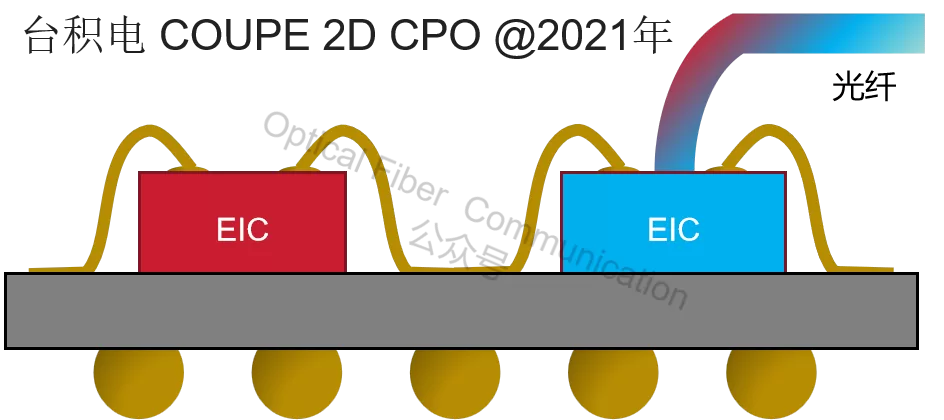
According to TSMC’s roadmap released in April this year, they plan to realize a 1.6T optical engine for pluggable optical modules in 2025, and then a 6.4T CPO optical engine based on CoWoS packaging technology in 2026.
Next, let us talk about 2.5D packaging, which is “0.5” D more than 2D and takes it a step further. 2.5D places all the chips side by side on an “interposer” layer.
The interposer is actually a very thin silicon or glass sheet filled with high-density wiring, as well as TSV or TGV.
Below is a schematic of TSMC’s 2.5D packaging based on an interposer.
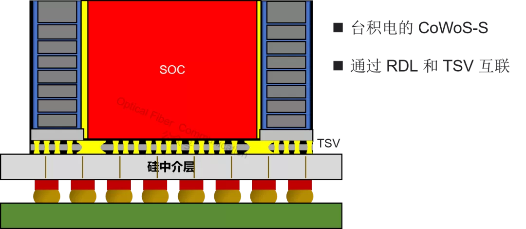
In CPO applications, 2.5D packaging also interconnects the PIC and EIC through silicon or glass interposers, which can minimize the length and complexity of the signal path.
Below is the glass-substrate CPO solution designed by Corning.
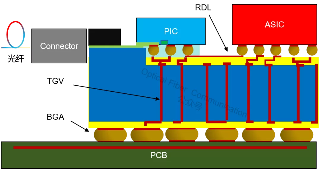
In this solution, the chipset is connected by fine copper lines and embedded in a single-side etched cavity. The PIC is connected to the optical fiber through a glass waveguide manufactured using ion-exchange technology.
To further improve the performance of the entire chip system, 3D integration technology was developed. Its main characteristic is to stack chips vertically in a single package, interconnected vertically through TSV, TGV, or micro-bumps.
Samsung’s X-Cube is a typical example. It integrates multiple logic chips and memory chips into a compact package using 3D stacking and vertical interconnect technology.
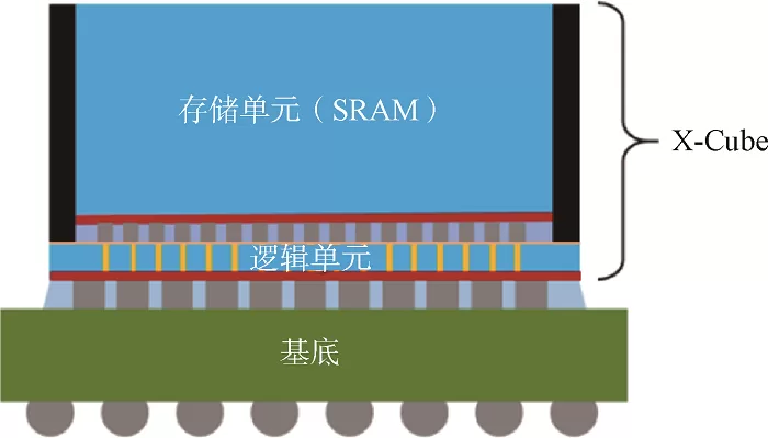
Similarly, 3D packaging is also applied in CPO. Optical components such as lasers, photodetectors, and modulators are integrated directly into the same package, forming a 3D stacked configuration with the electronic chips, thereby achieving minimal signal loss and power consumption.
Broadcom’s 3D CPO is a typical application, in which the PIC is a flip-chip placed on top of the EIC, connected to the ASIC through the substrate.
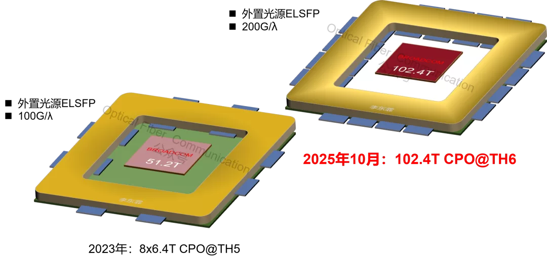
Broadcom: 51.2T CPO Reliability Data and 102.4T CPO Switch | Broadcom & HiSilicon: VCSEL NPO/CPO and Silicon Photonics CPO
In addition, in glass-based 3D CPO, the EIC, PIC, and glass are vertically stacked, with the ASIC mounted on the side. Intel states that this technology will be used for next-generation high-power processors. For more CPO-related knowledge and applications, please read:

Marvell’s Views on Scale Up/Out + 102.4T CPO Switch

NVIDIA: CPO External Light Source Coupling Scheme with Polarization Tracker
Thank you for reading! We invite you to join our community to obtain a large number of Ebooks, technical documents, and trend research reports in the fields of semiconductor chips / optical devices / optical modules!
Related Reading
- Marvell: Packaging Technology Evolution Path for Ultra CPO
- A CPO Optical Engine Packaging Structure with Pluggable Fiber
- CPO Packaging Structure Based on a Glass Carrier
Enjoy this article?
Subscribe to get new optical communication insights delivered to your inbox. Free, unsubscribe anytime.