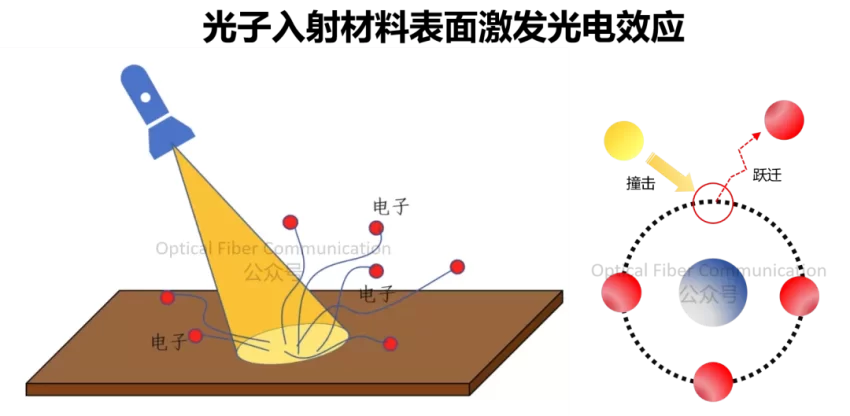
When discussing the technology or principles of modulators, photodetectors, and silicon photonics chips, we often mention the photoelectric effect and the electro-optic effect.
These two effects are both essentially changes in the energy and state of electrons/holes – a hole strictly corresponds to the absence of an electron. They only differ in the driving source (light/electricity) and their ultimate manifestations.
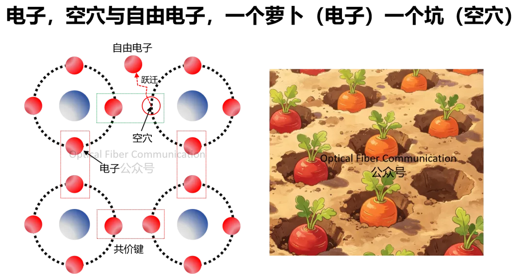
The photoelectric effect, simply put, is that when light shines on a material, electrons absorb photon energy and undergo energy level transitions, leaving a corresponding hole in the valence band.
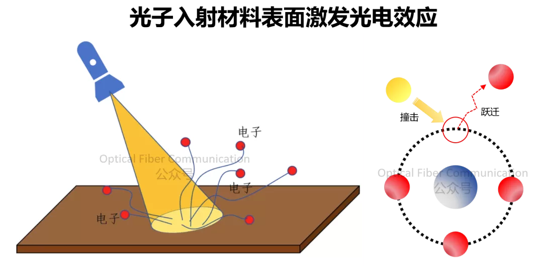
If the energy of the incident photon is large enough to exceed the material’s “work function”, the electron can break free from the material surface and escape, forming collectable photogenerated carriers. This is the core principle of photodetectors.
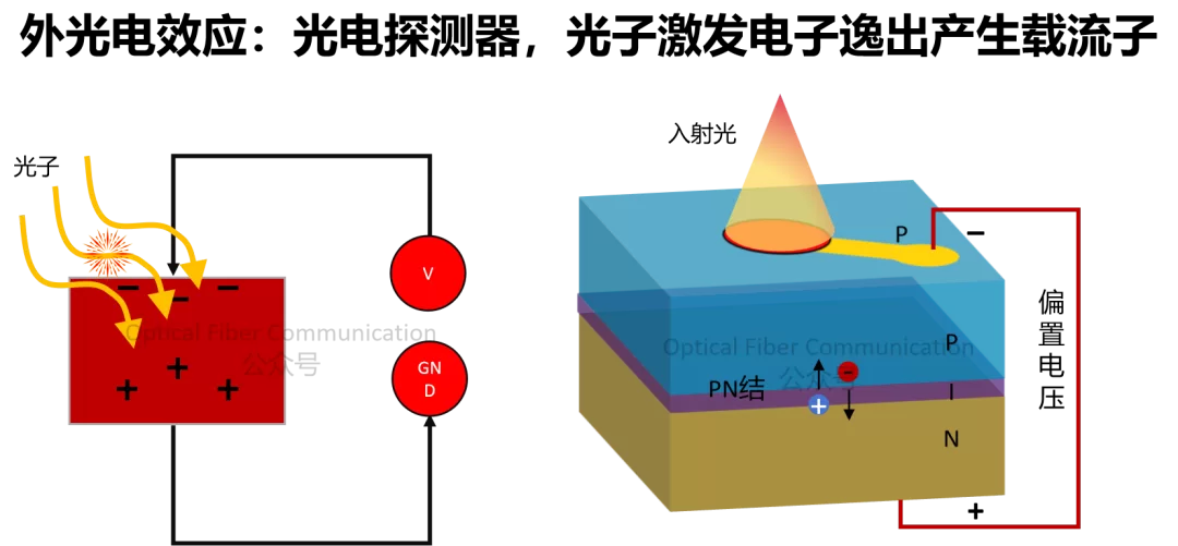
Basics: Detectors and Cutoff Wavelength
Huawei: C+L-Band 100G Bandwidth Germanium-Silicon Photodetector with Strain Layer
The work function mentioned here is the minimum energy threshold that an electron must cross to “escape” from the material surface, somewhat like a satellite needing to reach the second cosmic velocity to leave the Earth.
If the photon energy is not that strong – greater than the material’s band gap but smaller than the work function – then the electron cannot escape the material surface, and can only be excited from the valence band to the conduction band, forming free electron-hole pairs inside the material.
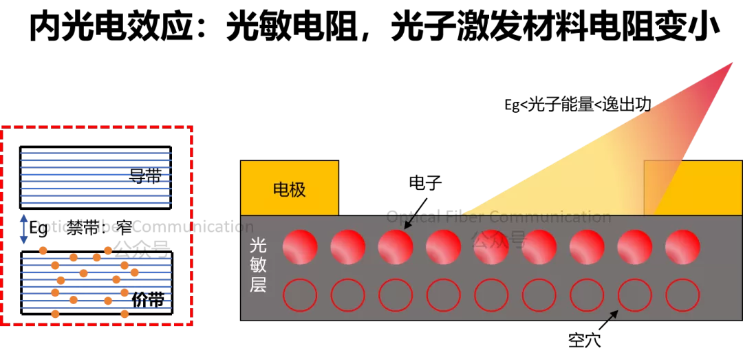
This change makes the material more conductive and lowers its resistance. Photoresistors work on this principle.
The electro-optic effect, on the other hand, is that an applied electric field changes the refractive index of the material.
In a silicon photonics modulator, the applied bias voltage changes the concentration of free carriers (electrons/holes) in silicon, and the change in carrier concentration directly affects the refractive index of silicon.
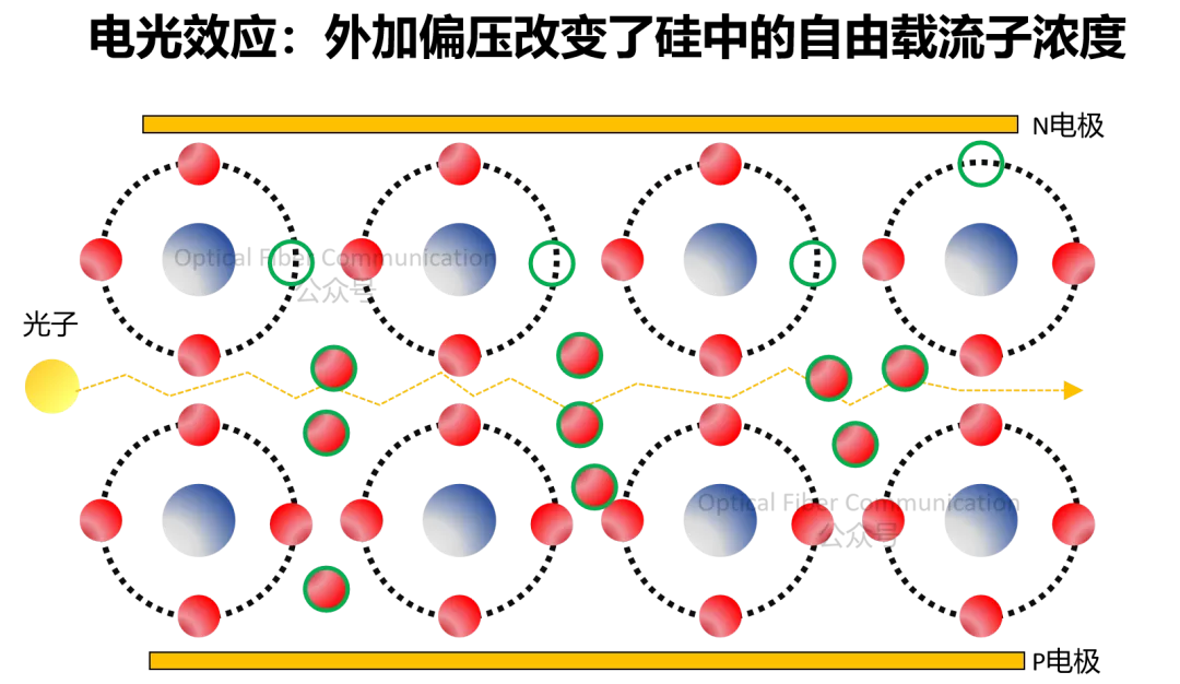
It can be understood this way: the more carriers there are, the greater the “resistance” to light, and the slower light travels in the material. The refractive index (n) is defined as the speed of light in vacuum divided by the speed of light in the medium.
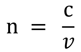
Since the refractive index has changed, the propagation speed of light in the waveguide will change. Over the same distance, whether light travels fast or slow, the waveform at the destination will be offset – this is called phase modulation.
Then, by placing the two phase-modulated light paths into an MZI interference structure, the phase difference is converted into a change in optical intensity, ultimately achieving the intensity modulation we need.
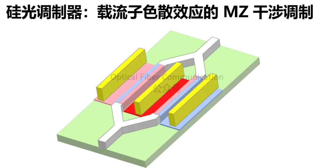
GlobalFoundries: 60GHz MZM Modulator Solution for 200G per Wavelength
Nokia: TFLN Two-Electrode Modulator Solution Supporting Single-Ended/Differential Driving
Lightmatter: 16-Wavelength 800G BiDi Microring Silicon Photonics CPO Solution
But note that not all “electrically controlled light” effects are related to carriers in silicon photonics. There is another class of material modulators whose electro-optic effect does not rely on carriers at all.
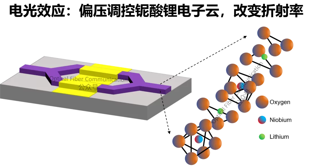
The most typical is the lithium niobate modulator. It relies on an applied electric field directly changing the polarization distribution of the electron cloud inside the crystal, known as the Pockels effect, thereby changing the macroscopic refractive index of the material.
A*Star: 8-Inch Silicon-Based TFLN 110GHz Modulator Mass Production Solution
Eoptolink: Single-Channel 400G TFLN 1.6T/3.2T Solution
HyperLight/Ciena: TFLN Process Progress and Coherent Lite 12.8T XPO Solution
The electro-optic effect of lithium niobate is like directly twisting the shape of a sponge with your hand: the external force (electric field) directly changes the structure of the material (electron cloud distribution), thereby changing the path through which light passes.
Because the entire process involves no free carriers and has no carrier lifetime limitation, the lithium niobate modulator responds much faster.
The silicon photonics modulator relies on an applied voltage to inject or deplete carriers and change carrier concentration. Although both it and lithium niobate’s classical electro-optic effect can electrically control light, their physical mechanisms are completely different.
So strictly speaking, silicon photonics’ carrier dispersion modulation does not quite count as the classical electro-optic effect.
Thanks for reading!
Please point out any inaccuracies.

If you are interested in semiconductors / optical components / optical modules / optical fiber communications
Welcome to follow us!
Related Reading
- Probabilistic Constellation Shaping (PCS) Technology (2)
- Does Data Center 800G Use PAM4 or Coherent Technology?
- Light and Technology: What’s the Deal with Nonlinear Effects in Optical Fiber?
Enjoy this article?
Subscribe to get new optical communication insights delivered to your inbox. Free, unsubscribe anytime.