In semiconductor manufacturing, silicon wafers serve as the basic material for mass-producing hundreds to thousands of integrated circuits. However, during volume production or prototyping, surplus wafers often occur.
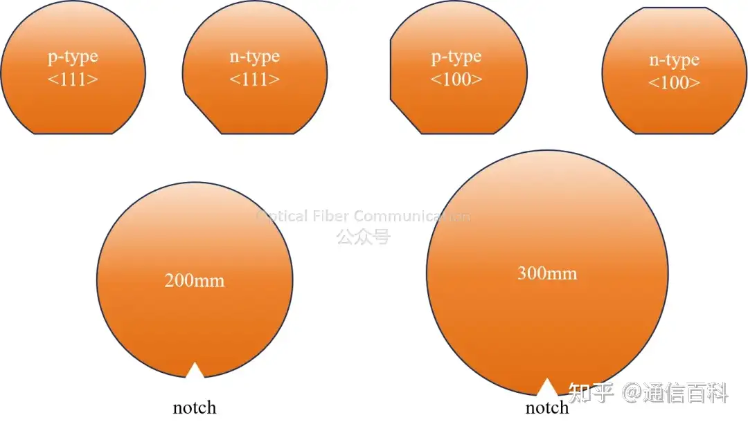
The causes of wafer surplus are diverse, involving multiple factors in both the manufacturing flow and business operations.
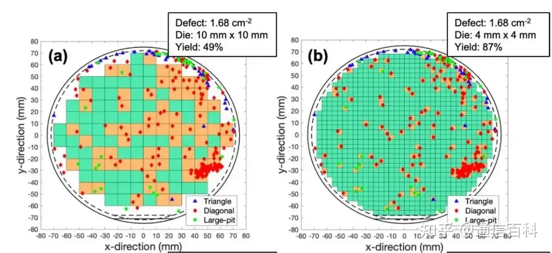
For example, during volume production, to reach the target shipment volume, companies usually produce a certain number of wafers in advance based on the expected yield (yield is not 100%) to compensate for losses caused by insufficient yield during production.
Yield, namely Yield, usually refers to the proportion of qualified chips in a batch of wafers that ultimately meet the design and functional requirements.

In addition, during prototype development or early production stages, some wafers may lose their purpose midway due to design changes or order cancellations, becoming surplus inventory.
Another common reason is the minimum processing batch size of the production line. For example, fabs usually use 25 wafers as the minimum unit for feeding materials, so even when actual demand is small, they have to produce more than needed. Meanwhile, test wafers and monitor wafers used for equipment debugging and process monitoring, although they account for about 20% of total silicon wafer shipments, are generally not used for product manufacturing after use, further increasing the surplus.
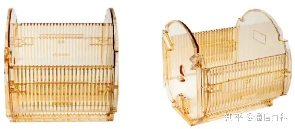
These surplus wafers can be classified and handled according to their process status and progress.
Many wafers are repurposed as test wafers, that is, monitor wafers, used to check equipment status and optimize process parameters, especially in key process steps such as ion implantation, chemical vapor deposition, etching, and chemical mechanical polishing, for pre-production condition debugging and particle control. After use, such wafers can also be recycled through processes such as acid cleaning and stripping, allowing multiple reuse.
Related Reading
- How to Couple VCSEL Light into the PIC Wafer Plane?
- Is This Wafer-Level Packaging?
- What Exactly Is the Relationship Among Wafer, Silicon Wafer, Bare Die, and Chip?
Enjoy this article?
Subscribe to get new optical communication insights delivered to your inbox. Free, unsubscribe anytime.