Reactive Ion Etching, also called RIE, is a process in semiconductor manufacturing for etching structures into thin films.
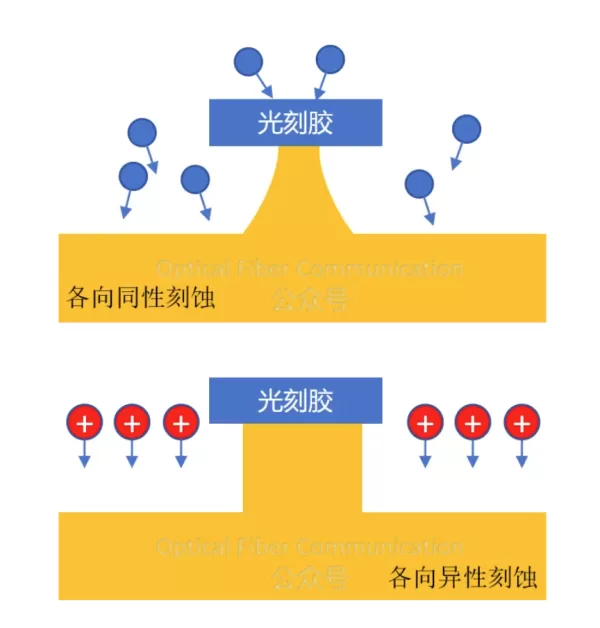
RIE can perform both isotropic etching (etching roughly equally in all directions) and anisotropic etching (mainly etching downward), as shown in the schematic below. It has this capability because RIE combines chemical reactions and physical bombardment.

Let me briefly describe the process: the wafer is placed on the high-frequency electrode of the process chamber. The gas is ionized to produce a plasma containing free electrons and positive ions. When the high-frequency electrode is momentarily positively charged, electrons are attracted to its surface and accumulate, forming a high negative charge, that is, the bias voltage. The heavier ions respond with a lag and, under the average electric field, are attracted by this negatively charged electrode.


If these ions have a relatively long mean free path (fly far before colliding), they will strike the wafer surface almost vertically. This impact has two effects:
First, high-speed ions directly “knock” the surface material off (physical sputtering); second, the active chemical species (free radicals) in the plasma also react with the surface material (chemical etching).
Therefore, RIE is sometimes also called ion-enhanced etching or reactive ion etching.
Because the ions basically strike vertically, the wafer sidewalls are not directly hit, thus avoiding lateral etching, which produces a vertical, steep profile (anisotropic).

RIE’s selectivity is usually moderate. Although physical sputtering helps vertical etching, it is not very material-selective, which limits the high selectivity that chemical etching can achieve. Also note that high-energy ion bombardment may damage the wafer surface, and this damage usually needs to be repaired later by thermal annealing.
When etching silicon, to achieve high anisotropy, a technique called “sidewall passivation” is commonly used.
The specific approach is to introduce a little oxygen (O₂) during etching. The oxygen reacts with the silicon atoms sputtered from the silicon surface at the sidewalls, forming a very thin layer of silicon dioxide (SiO₂). This silicon dioxide layer acts like a protective layer covering the vertical sidewalls, blocking lateral chemical etching. On the horizontal bottom, the continuous ion bombardment keeps knocking off this oxide film, so etching can keep going downward.

The etching rate is affected by many factors, such as chamber pressure, the power applied to the high-frequency electrode, the type of process gas used, the gas flow rate, and the wafer temperature. The degree of etching anisotropy generally increases as the high-frequency power increases, the chamber pressure decreases, or the wafer temperature decreases.
Finally, selectivity and etching rate largely depend on which process gas you choose. For etching silicon and its compounds (such as silicon dioxide and silicon nitride), gases containing fluorine (such as CF₄, SF₆) and chlorine (such as Cl₂, BCl₃) are mainly used.
Thank you for reading!
We can provide AOC/DAC/MPO cables, optical modules, and optical transceivers at various rates, as well as various optical components used in them, such as aspheric lenses, collimating lenses, aspheric lens arrays, and wave plates, and we can also provide custom development services. Welcome to contact us via WeChat WaytoICT, email: mark@bitwavx.com.
Related Reading
- Structure and Principle of Common Dry Etching Equipment for MEMS
- What Is Strained-Layer Epitaxy?
- What Is the Difference Between a Semiconductor Substrate and an Epitaxial Layer?
Enjoy this article?
Subscribe to get new optical communication insights delivered to your inbox. Free, unsubscribe anytime.