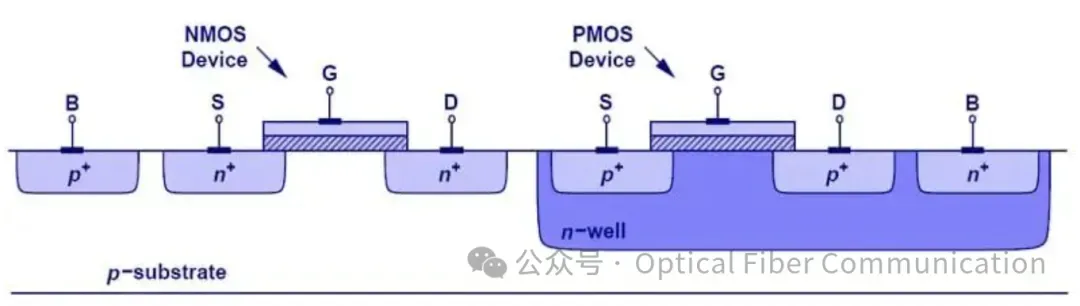
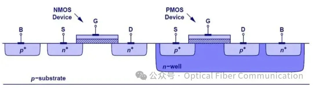
CMOS, namely Complementary MOSFET, is composed of PMOS field-effect transistors and NMOS field-effect transistors in a symmetric and complementary form, so it is also called complementary MOSFET. CMOS can be said to be the cornerstone of modern integrated circuits.
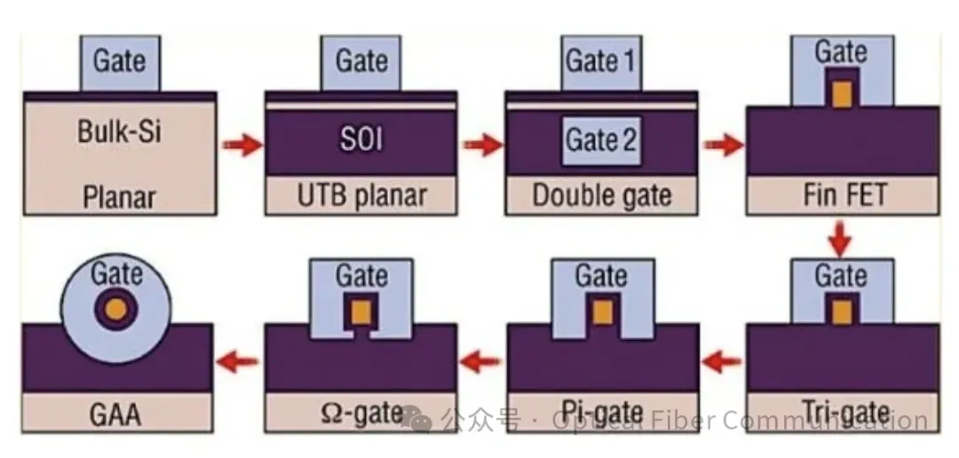
Over the past 20 years or so, CMOS technology has made significant progress. The following is the evolution of CMOS, from double-gate, triple-gate, π-gate, ω-gate to gate-all-around…..
Looking at FinFET from the evolution of MOSFET: because the channel is vertical and looks like a fin, it is called a fin field-effect transistor. Since 2011, the first batch of chips using FinFET came out, bringing semiconductors into sub-25nm processes. In 2012, the first commercial 22nm FinFET was born. Its performance has been continuously improved and enhanced since then.
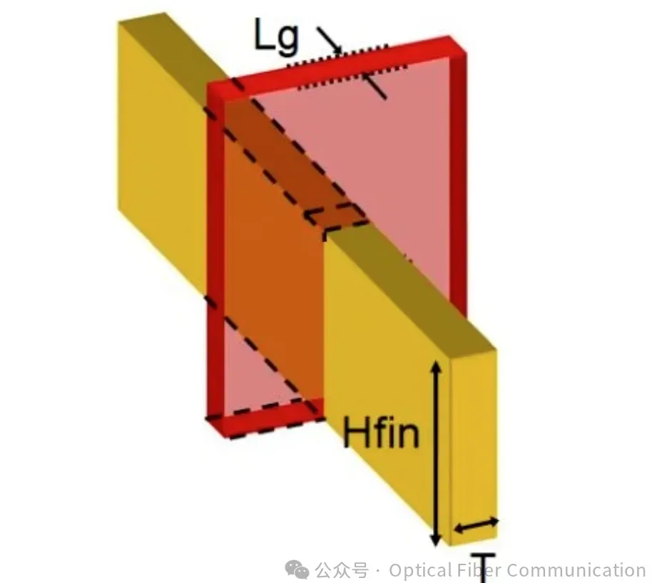
Figure: FinFET structure
We know that FinFET can suppress the short-channel effect better than MOSFET, thereby enabling transistor scaling, so FinFET replaced MOSFET. But FinFET is not omnipotent either! As device dimensions keep shrinking and performance requirements rise, because there is not enough electrostatic control, leakage and signal-interference problems become increasingly prominent, especially after 10nm, and after 5nm it is no longer useful. So, we cannot help but ask, is FinFET now approaching its end? Let us first look at what drawbacks FinFET currently has. At 10nm and below, the main problems FinFET faces are:
- Short-channel effect: as the channel length shortens, control between the source and drain weakens, leading to increased leakage current and higher static power consumption.
- Threshold-voltage drift: due to quantum effects, as the gate length continues to shrink, the effective control of the gate over the channel decreases, causing the threshold voltage to become unstable.
- Area efficiency: although FinFET’s three-dimensional structure increases drive current compared with planar MOSFET, continuing to shrink the fin height and width will bring manufacturing challenges and performance degradation.
- Corner effect: compared with the electric field at the sidewall, the electric field at the corner is always amplified.
- Quantized device width: fractional fins cannot be made; device dimensions can only be specified as integer multiples of a full fin.
Of course, there are also cost and manufacturing reasons. Therefore, GAA (Gate-All-Around), namely gate-all-around transistor technology, has been proposed to solve these problems encountered by traditional FinFET. The specific underlying principle is: GAA technology wraps the gate material around all four sides of the channel, which can better control the charge movement in the channel. The structure of GAA is shown in the right half of the figure below: it can be seen that the GAA gate is in contact with the channel on all four sides, thus providing better current control. This is similar to what FinFET did relative to the MOSFET architecture back then.
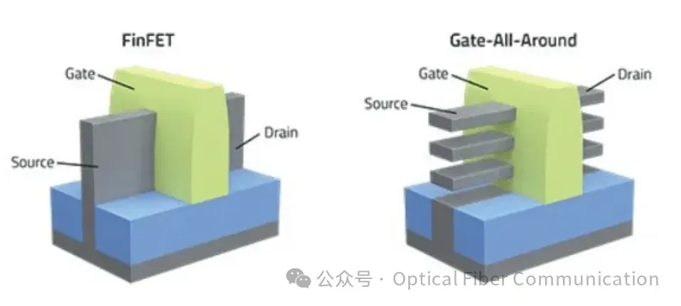
Figure: FinFET and GAA
But at present, GAA technology is still relatively new. It is understood that Intel has already incorporated it into its roadmap. As for whether it will become the next-generation technology, let us wait and see.
Related Reading
- How to Couple VCSEL Light into the PIC Wafer Plane?
- What Is Strained-Layer Epitaxy?
- 2024 Semiconductor Industry Research Report – Automotive-Grade Chips
Enjoy this article?
Subscribe to get new optical communication insights delivered to your inbox. Free, unsubscribe anytime.