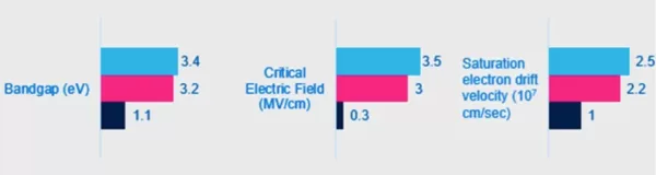
Gallium nitride and silicon carbide both belong to a class of materials called wide-bandgap (WBG) semiconductors. The energy difference between the highest occupied state of the valence band and the lowest unoccupied state of the conduction band is called the bandgap, and it represents the electrical conductivity of the material. In plain terms, the energy difference represented by the bandgap is the minimum energy required to make a semiconductor go from insulating to conducting. A larger bandgap means more energy is needed to excite valence electrons into the conduction band. Conversely, when the valence band and conduction band overlap like in metals, electrons can easily jump between the two bands, meaning the material is classified as a conductor.

The difference between conductors, insulators, and semiconductors can be represented by the bandgap width. The bandgap width of insulators is usually greater than 5 eV; the bandgap width of semiconductors is usually less than 5 eV; in conductors, the valence band and conduction band overlap, making their bandgap zero.
The bandgap of a semiconductor allows only a small number of the material’s valence electrons to enter the conduction band. This characteristic makes its conductivity between that of conductors and insulators, which is partly why semiconductor materials are suitable for circuits—because they do not cause short circuits like conductors. The bandgap widths of silicon and gallium arsenide are 1.1 eV and 1.4 eV respectively, while those of silicon carbide and gallium nitride reach 3.2 eV and 3.4 eV respectively. Power devices made of wide-bandgap semiconductors (2~4 eV) are often able to operate at high voltage, high temperature, and high frequency.
Comparison of five performance parameters
In addition to the bandgap width, the other important material performance parameters are: critical breakdown field strength, saturation electron drift velocity, electron mobility, and thermal conductivity.

Critical breakdown field strength is the maximum voltage that can be applied to a device before avalanche breakdown occurs. Avalanche breakdown occurs when the electric field strength is large enough to tear valence electrons away from their parent atoms. Silicon carbide and gallium nitride both have relatively high breakdown field strengths, at 3.0 MV/cm and 3.5 MV/cm respectively. This means that silicon carbide and gallium nitride can withstand more than ten times the voltage of silicon, or they can also support lower voltages with smaller-sized devices.
Saturation electron drift velocity is the maximum velocity electrons can reach under a high electric field in a semiconductor material. A higher saturation electron drift velocity means that a given device can operate at higher frequencies and achieve faster switching.
Electron mobility is the average velocity of electrons under a unit electric field, and is a measure of how fast electrons are pulled (or pushed) by an electric field as they travel through the semiconductor. The larger the electron mobility, the smaller the resistivity; when passing the same current, the power consumption is lower, which also means greater current-carrying capacity.
One of the notable differences between gallium nitride and silicon carbide is electron mobility. First, the electron mobility of silicon is 1450 cm²/Vs, and that of gallium nitride is 2000 cm²/Vs, meaning electrons in gallium nitride move more than 30% faster than in silicon. However, the electron mobility of silicon carbide is only 900 cm²/Vs, which is 45% of that of gallium nitride. With its high electron mobility and high saturation electron drift velocity, gallium nitride has become the material of choice for high-frequency devices.

Thermal conductivity characterizes the ability of a material to transfer heat through itself. Considering the application environment of semiconductor materials, thermal conductivity directly affects the material temperature. In high-power applications, the low efficiency of materials often generates heat, thereby raising the material temperature and subsequently changing its electrical characteristics. The thermal conductivity of gallium nitride is 1.3 W/cmK, which is even worse than silicon. However, the thermal conductivity of silicon carbide is 3.8 W/cmK, making it outstanding in improving heat-transfer-load capability. This characteristic gives silicon carbide a great advantage in high-power devices and high-temperature applications.
In addition to the five material performance parameters introduced above, compared with silicon, manufacturing cost limits the economies of scale of gallium nitride and silicon carbide, making these two materials more expensive in the short term. Silicon carbide may be the material that can quickly break through the cost constraint, because it is easier than gallium nitride to manufacture larger and more uniform single-crystal wafers. For gallium nitride, considering cost factors, silicon is usually chosen as the substrate. However, since the thermal mismatch and lattice mismatch between silicon and gallium nitride are severe, this low compatibility means that a gallium nitride epitaxial layer cannot be directly grown on a silicon substrate, and multiple buffer layers (aluminum nitride) need to be grown for transition. Therefore, the epitaxial layer quality is much worse than that of silicon carbide, and the yield is also lower.
However, over time, given its higher electron mobility, gallium nitride will find its place in small high-frequency products. Silicon carbide is more preferable in high-power products because it has better thermal conductivity than gallium nitride. Taken together, gallium nitride and silicon carbide each have their own advantages and disadvantages in material performance, and their application fields also have different emphases and are complementary.

Currently, gallium nitride devices are commonly used in high-frequency products related to chargers, base stations, and 5G communications. Silicon carbide has great application potential in electric vehicles, EV charging infrastructure, solar energy, offshore wind power, and other green-energy power-generation equipment. These two materials actually have different optimal voltage levels. Silicon-based gallium nitride (GaN-on-Si) can make use of existing silicon-wafer manufacturing equipment, but the voltage is usually limited to within 650 V. It is currently mainly used for low-power RF devices, especially widely applied in consumer-electronics fast-charging products, with a strong trend of replacing Si MOSFETs. Since 5G base stations use multiple-input multiple-output antenna array solutions, gallium nitride RF devices greatly improve the power consumption and size of the entire antenna system, so 5G communications will be the main growth driver of the gallium nitride RF device market.
By contrast, silicon carbide devices are designed for voltages of 650 V and above. Especially at voltages above 1200 V, silicon carbide becomes the best solution for various application fields. Applications such as solar inverters, EV chargers, and industrial AC-DC will migrate to silicon carbide in the long run. Among them, new-energy vehicles are the main growth driver of the silicon carbide power-device market, with the main application directions being traction inverters, high/low-voltage DC-DC converters, and on-board chargers.
We are currently in the early development stage of the wide-bandgap semiconductor industry. However, with global policy support in recent years for urban infrastructure, new energy, energy conservation, and environmental protection, the demand for high-performance power devices is bound to increase. Therefore, it is believed that in the future, both silicon carbide and gallium nitride will certainly play a more important role than now and integrate into their respective commercial markets.
Related Reading
- 2024 Semiconductor Industry Research Report – Automotive-Grade Chips
- 2024 Global and Taiwan Semiconductor Industry Outlook
- What Is the Difference Between a Semiconductor Substrate and an Epitaxial Layer?
Enjoy this article?
Subscribe to get new optical communication insights delivered to your inbox. Free, unsubscribe anytime.