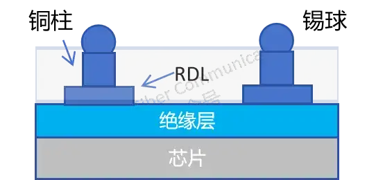
In the traditional chip manufacturing and packaging flow, chips are first fabricated on the wafer, then cut into individual dies and packaged to protect them from physical damage and provide electrical connections.
Moving the packaging step earlier to the wafer stage – packaging the chips directly on the wafer and eliminating the steps of dicing and individual packaging – is called Wafer-Level Packaging, abbreviated as WLP. Below, let us briefly look at the WLP process for reference. Note that the actual manufacturing process may vary depending on the specific application. First, wafer fabrication is carried out to produce the required integrated circuits.
The wafer
First, rewiring is performed on the wafer, that is, additional metal layers, copper pillars or conductive paths are formed on the wafer to create vias and a redistribution layer (RDL), ensuring that each die unit can effectively connect with external circuits. Then copper pillars are formed, and bumps are generated on top of the copper pillars.
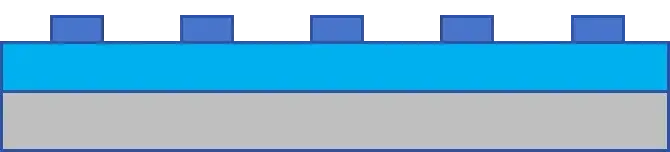
Rewiring to form copper pillars
Next, the wafer is coated with a layer of resin. This resin material not only provides protection but also offers good electrical insulation.

Resin sealing
After resin sealing, the contact points of each die unit on the wafer are implanted with solder ball pins, so that electrical connections can be established with the circuit board or other electronic components in the subsequent assembly process.
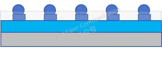
Solder ball bumps
Finally, the fully packaged wafer is cut into individual dies through a dicing process.
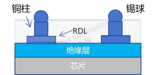
Dicing into dies. Simply put, the difference between WLP and traditional packaging is that traditional wafer packaging is dicing first and then packaging and testing, with the packaged size about 20% larger than the original die size.
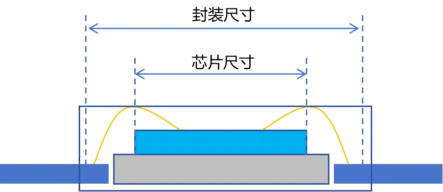
Traditional packaging. WLP, on the other hand, first performs packaging and testing on the entire wafer, and only then dices and separates. Therefore, the packaged volume is almost the same as the actual die size.
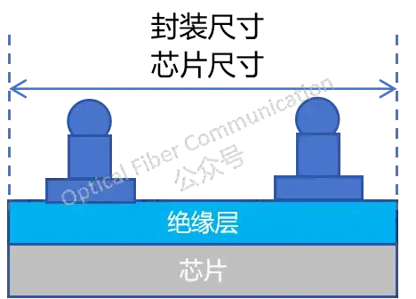
WLP packaging. Overall, the advantage of WLP is that it can achieve a smaller package size and higher integration. At the same time, because the packaging process is completed at the wafer level, it can also greatly reduce production cost and time.
Thanks for reading!
Published with authorization from the OFC official account. You can follow the OFC official account:
Related Reading
- How Did the Road from OTN to Flexible FlexO Packaging and Multiplexing Unfold?
- How to Couple VCSEL Light into the Plane of a PIC Wafer?
- What Are the Packaging Processes for Optical Modules?
Enjoy this article?
Subscribe to get new optical communication insights delivered to your inbox. Free, unsubscribe anytime.