
Since Soref and Bennett first revealed the correlation between carrier concentration and refractive index change in silicon materials in 1987, this discovery has opened a new path for optical modulation technology. By adjusting the carrier concentration in silicon devices, the propagation characteristics of light waves can be effectively regulated, thereby achieving precise modulation of optical signals.
Based on this effect, researchers have designed key optoelectronic devices such as high-speed PN junction optical modulators, as shown in the figure below:
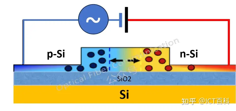
Specifically, the changes in silicon’s refractive index and absorption are closely related to the concentrations of electrons and holes. The relationship between refractive index and carrier concentration change:
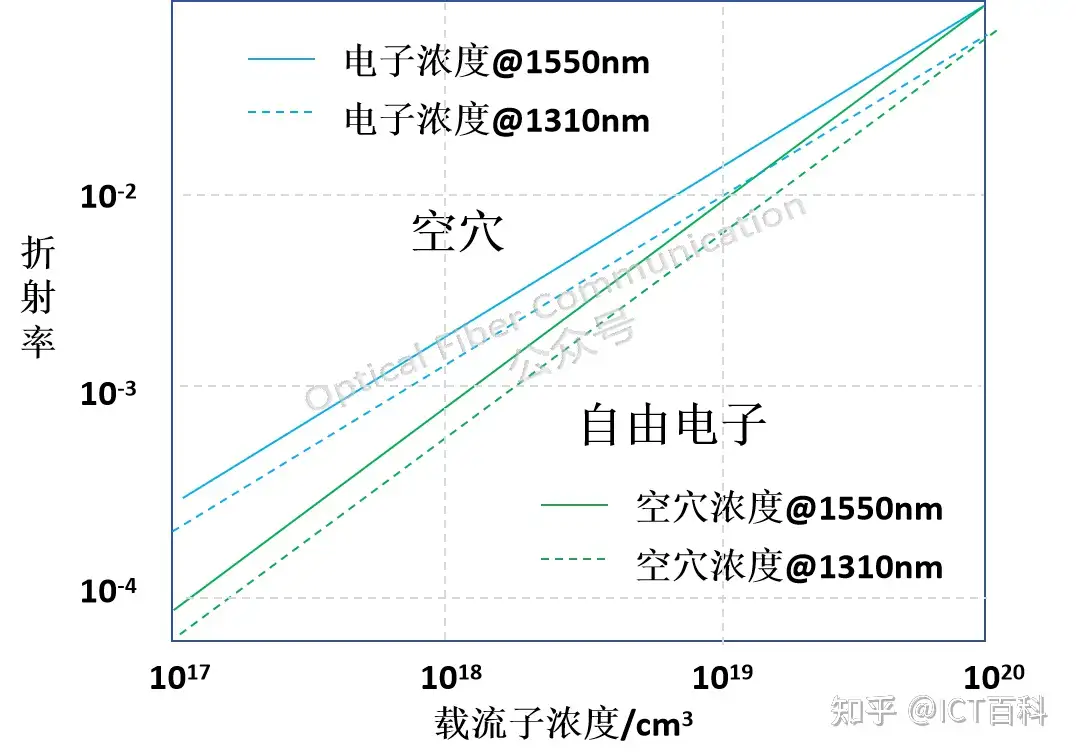
- The refractive index change of holes is larger than that of electrons.
The relationship between absorption and carrier concentration change:
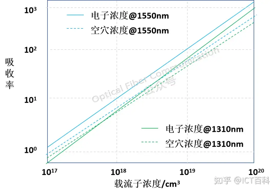
- The absorption of holes is lower than that of electrons.
From the figures above, we can also summarize: compared with electrons, holes exhibit lower absorption characteristics while causing more significant refractive index changes. Furthermore, when considering wavelength dependence, both refractive index and absorption change with the square of the wavelength. This characteristic makes holes highly favored in optical modulator design, especially in biased junction designs such as Mach-Zehnder modulators and microring modulators. For the PN junction above, the effective refractive index and optical transmission loss are also related to the bias voltage. As the reverse bias voltage increases, the effective refractive index increases and the optical transmission loss decreases.
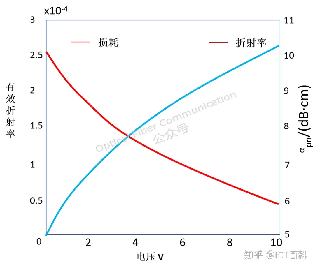
This is because the carrier concentration in the waveguide region decreases, and the applied voltage is almost removed, causing the depletion region to widen. In addition, the resistance R and capacitance C of the PN junction are also very important factors of the device, which can affect the size of the 3dB cutoff frequency f. The calculation formula is as follows:
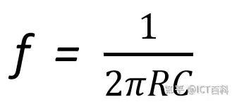
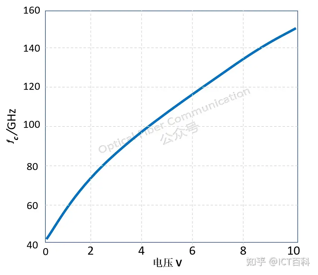
If the capacitance C decreases, then under the same applied voltage, the charge in the depletion region can be redistributed more quickly, allowing the depletion region to expand or contract more quickly. If the resistance R decreases, it means current flows more easily in the depletion region, which also promotes the expansion of the depletion region because charge can move faster from one side of the PN junction to the other. All of this means the depletion region will widen. At the same time, we can see from the figure below that the cutoff frequency increases as the applied DC voltage increases, and the frequency response of the PN junction can easily exceed tens of GHz.
However, when using a long PN junction (large capacitance C) and a large source impedance R (such as 50 ohms), RC becomes the limiting factor. This is also the basic principle of Mach-Zehnder modulators or phase shifters. To avoid the RC limitation, techniques such as traveling-wave electrodes are needed to match the group velocity of the RF signal with that of the optical wave.
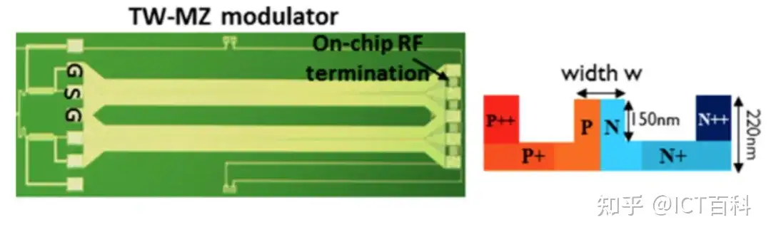
However, the resistance of the PN junction can be reduced by optimizing the doping concentration and the distance between the dopant and the junction. Specifically, minimizing the distance from the contact point to the junction will reduce the RC time constant. Considering the optical transmission loss of the doped contact, the typical doping concentration is around 1e18 cm^-3. Because the junction capacitance of a reverse-biased PN junction is small, with a typical value of 0.2-0.8pF/mm, the modulation efficiency of depletion-type modulators is not high, with a typical Vpi*L value of 1.5-2V*cm.
Therefore, to improve modulation efficiency, researchers have made many innovations in the structure of PN junctions, such as interleaved, L-shaped, and U-shaped structures.
- Interleaved doping
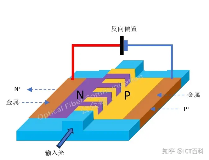
In this design, P-type and N-type doped regions are alternately arranged along the propagation path of the waveguide, creating a depletion region extending along the propagation direction. This layout increases the overlap between the waveguide mode and the depletion region, thereby optimizing the light-matter interaction and effectively improving modulation performance.
- L-shaped doping
Using a specific ion implantation technique, this design constructs the PN junction in the vertical direction, which increases the surface area of the PN junction capacitance and thus the capacitance value, helping to improve modulation efficiency. The figure below shows the structural characteristics of the L-shaped PN junction.

- U-shaped doping
The structure diagram below shows the design of the U-shaped PN junction, where the layout of the P-type and N-type doped regions presents a U shape. This structure can achieve higher modulation efficiency because of its larger junction capacitance. Thanks to the larger overlap integral between the depletion region and the waveguide mode, the transmission loss of this structure is reduced.

The optimization of these structures helps improve modulation efficiency while maintaining high modulation bandwidth and low power consumption. Thanks for reading. If there are any inaccurate expressions, please point them out!
Related Reading
- It Is This Simple: Mach-Zehnder M-Z Modulator
- Ge Electro-absorption Modulator
- Nvidia: Design Approach of High-Speed Microring Modulators for Single-Channel 200G+
Enjoy this article?
Subscribe to get new optical communication insights delivered to your inbox. Free, unsubscribe anytime.