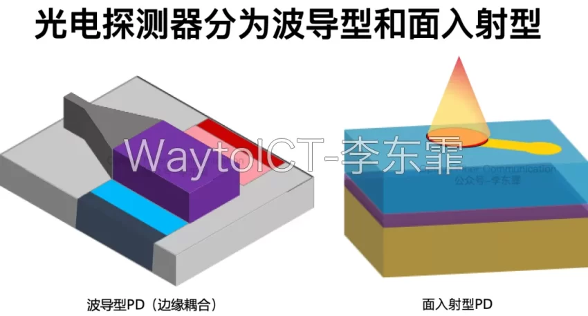
A few days ago, in the article “AMD: Electro-Optical Co-Design and Key Trade-Offs of CPO Optical Transceivers“, it was mentioned that to minimize the input capacitance entering the TIA, a waveguide photodetector should be chosen.
According to the way light is incident, photodetectors can be divided into surface-illuminated photodetectors and waveguide photodetectors.
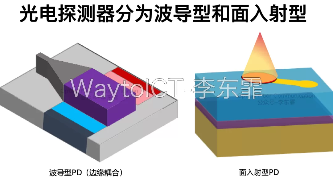
Surface illumination means that light enters the absorption region from the front or back of the detector. After photons are absorbed, electrons in the valence band transition to the conduction band, generating electron-hole pairs, which form a photocurrent under the action of the electric field.
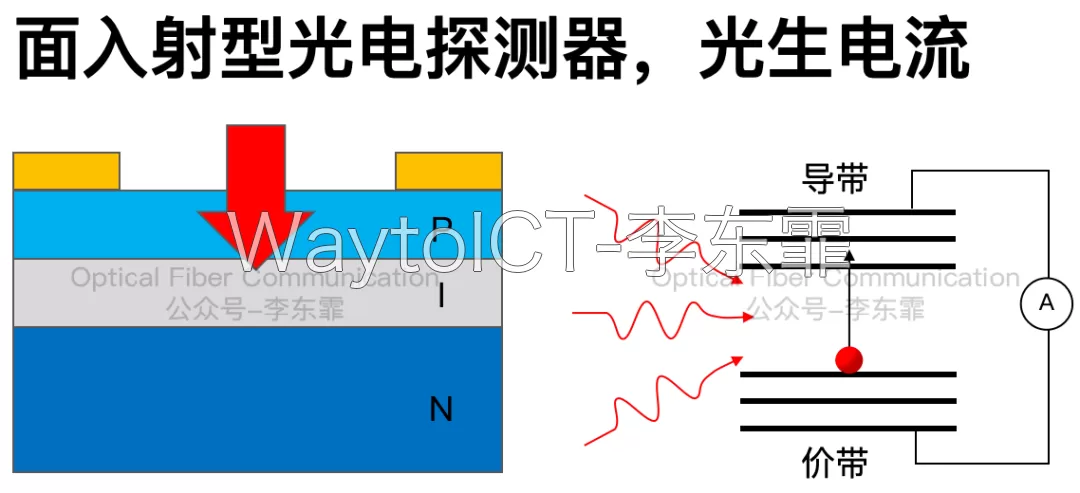
For a general PIN junction detector, the responsivity and bandwidth are affected by the thickness of the intrinsic I region, the junction capacitance, and the carrier transit time.
The thicker the I region, the more complete the absorption, but the longer the carrier transit time; the junction capacitance and RC time constant also limit the bandwidth.
The I-region absorption materials of surface-illuminated detectors generally include Si, InGaAs, and Ge, with thicknesses mainly ranging from several hundred nm to 3 μm.
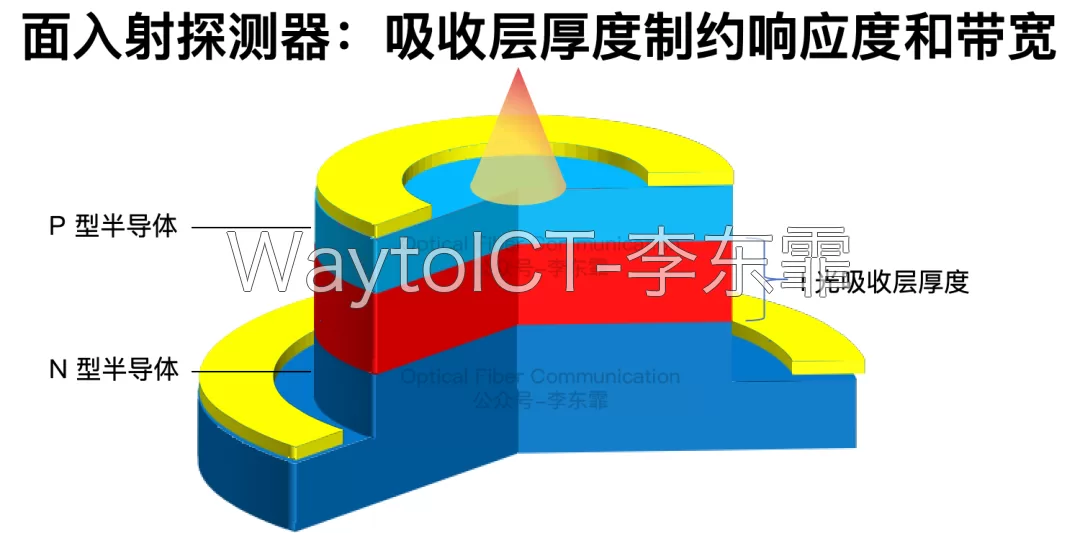
For high speed, the absorption region is made thin, such as in silicon-germanium Ge-on-Si surface-illuminated detectors; for high responsivity, the absorption region is made thick, but the bandwidth will drop.
But to balance high responsivity, the absorption layer thickness cannot be reduced indefinitely, as this brings a larger junction capacitance, increases the TIA input capacitance, and affects the performance of the backend TIA.
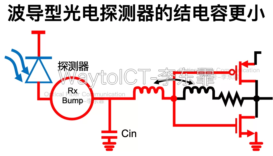
To minimize the input capacitance entering the TIA, a waveguide photodetector can be chosen. Compared with surface-illuminated PDs, waveguide PDs have smaller junction capacitance.
Waveguide detectors can be divided into edge-coupling and evanescent-coupling types. At present, the most common and mature scheme uses germanium (Ge) as the absorption region material.
Edge coupling differs from surface-illuminated detectors: the silicon waveguide end face is directly aligned with the Ge absorption region, and light enters the Ge from the waveguide end face.
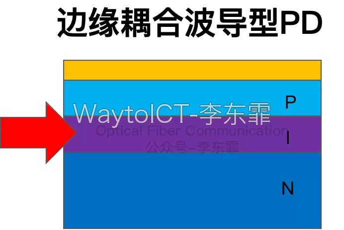
Light propagates along the waveguide, and the current direction is generally perpendicular to the light propagation direction. The light is continuously absorbed by the absorption layer during propagation.
Since the absorption of a waveguide detector proceeds along the waveguide direction, the absorption length can be made much larger than that of a surface-illuminated detector.
But its optical coupling area is smaller, with mode field mismatch, lower coupling efficiency, and increased difficulty in coupling with optical fiber.
A tapered mode spot-size converter can be integrated between the waveguide and the absorption region to smoothly transform the optical field. For example, Sumitomo’s coherent receiver PD uses a two-step tapered structure.
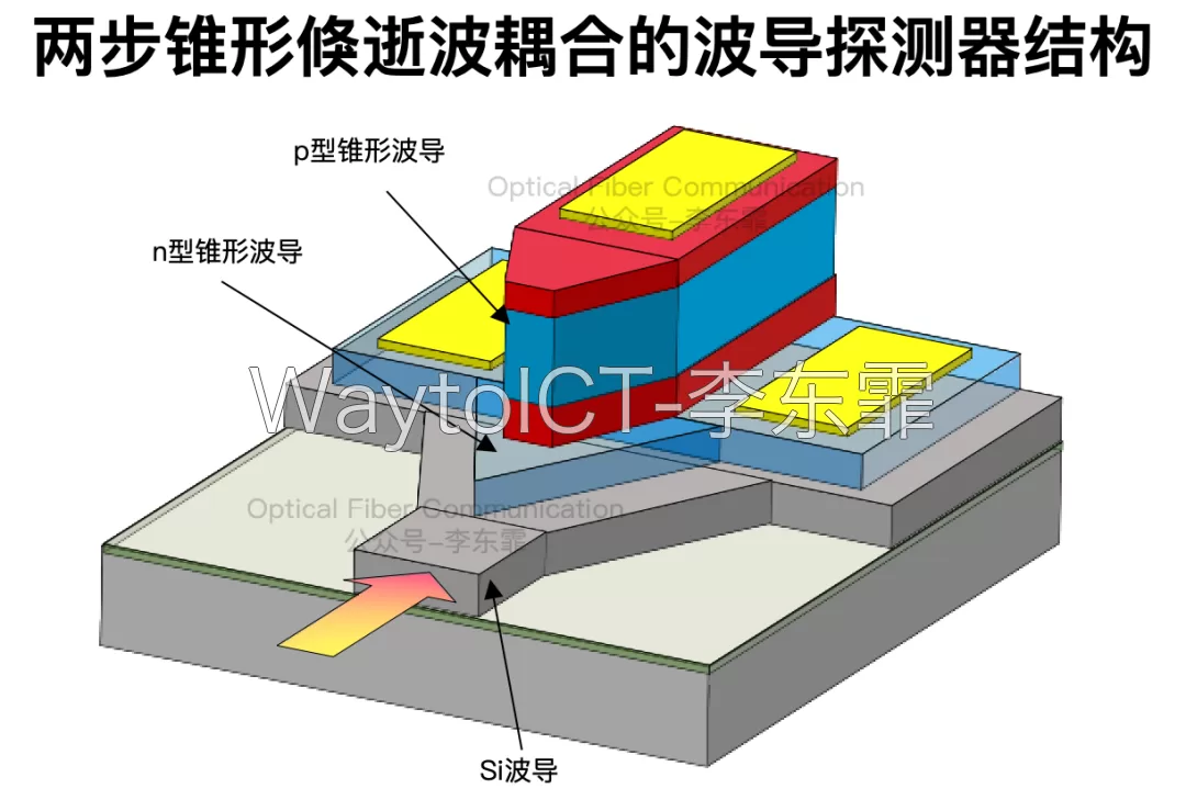
Related reading: Sumitomo: Silicon-Based and InP Hybrid-Integrated Coherent Receiver
Evanescent coupling can also reduce coupling loss and improve waveguide coupling efficiency, and is currently a commonly used coupling scheme for waveguide detectors.
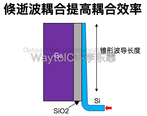
In terms of coupling structure, a refractive index gradient can also be used to increase the optical coupling area.
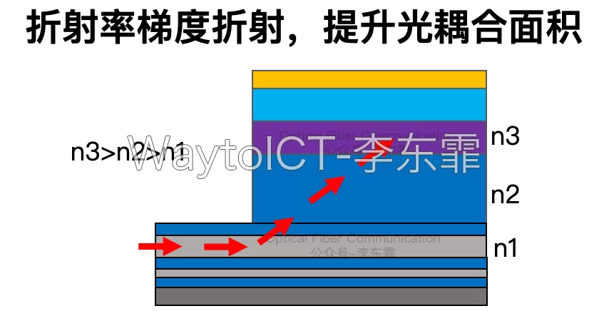
Besides the coupling structure, the electrode design also affects the responsivity. The detector’s electrode structure can be optimized, for example by reducing the electrode size and opening holes in the electrode, to reduce blocking and improve the electric field distribution, thereby improving the responsivity.
Thanks for reading,
Please forgive any inaccuracies!
The compilation report on Optical Chips, Optical Devices, and Optical Transceivers (OFC2026), printed in color and bound in A4, consists of two volumes totaling 525 pages, about 200,000 characters. If you need it, welcome to contact us to order, at a favorable price!
WeChat contact: WaytoICT
Further Reading
- Fundamentals: Uni-Traveling-Carrier Photodetectors (UTC-PD)
- Fundamentals: Photoelectric Effect and Electro-Optic Effect
- Huawei: C+L Band 100G Bandwidth Germanium-Silicon Photodetector with Stress Layer
- Fundamentals: Eye Diagram
- What Is EML? The Working Principle, Applications, and Evolution of Electro-Absorption Modulated Lasers (EML)
- Coherent: Traveling-Wave Electrode High-Speed EML Scheme (Paid Column)
Enjoy this article?
Subscribe to get new optical communication insights delivered to your inbox. Free, unsubscribe anytime.