The optical transceiver is the core device in an optical fiber communication system, and is the optoelectronic device that realizes optical-electrical conversion and electrical-optical conversion during optical signal transmission. In terms of layering, it belongs to the physical layer of the OSI model.
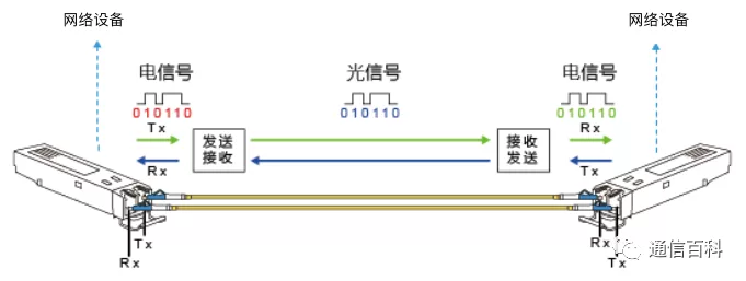
So where are optical transceivers mainly used? Basically all network transmission links involve optical transceivers. I will briefly sort out their application scenarios as follows:
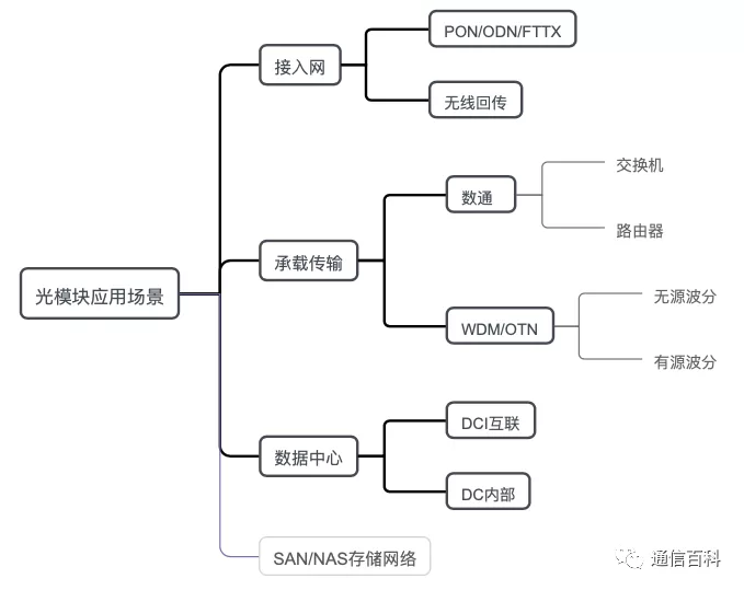
Optical transceivers are mainly used in the telecom market and the datacom market, with shipment volumes at the millions or even tens of millions level, and a relatively fast pace of iteration.
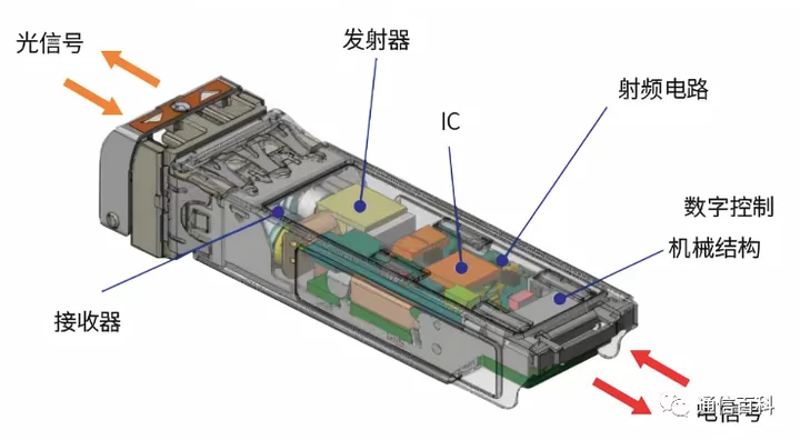
Therefore, the structure and design of optical transceivers in these scenarios are not the same, in order to meet the needs of different customers. Below we look at a relatively typical non-hermetic optical transceiver structure. As shown in the figure below, it mainly consists of optoelectronic devices (optical transmitter, optical receiver), functional circuits, and optical interfaces.
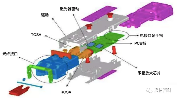
Inside these optical devices, the packaging methods mainly include hermetic packaging and non-hermetic packaging. The following components inside the package mainly include:
- LD – Laser Diode
- PD – Photodetector
- Amplifier (TIA, LA, AGC)
- CDR – Clock Data Recovery
- Driver – Driver Chip
- Mux&DeMux (multi-channel optical transceivers)
I have sorted them out with a mind map as follows:
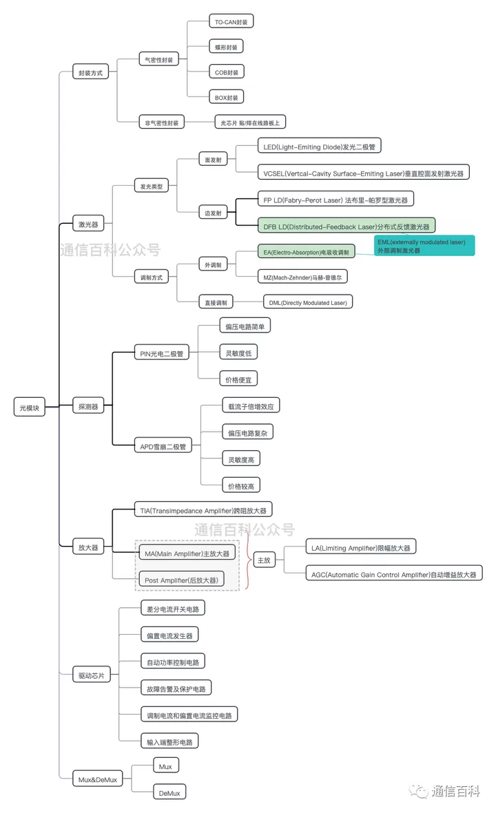
Let’s first look at the packaging methods, considering the different application environments of optical transceivers. In places easily corroded by water vapor and greatly affected by temperature, hermetic packaging is used, sealing the optical chip in a metal shell with a sealing window filled with inert gas. In indoor equipment rooms with better temperature control, the lower-cost non-hermetic packaging method is used. TO-CAN Packaging
The full English name is Transistor Outline Can, where “Transistor” means transistor and “Can” means a container. CAN serves as this container, used to mount optical chips such as VCSEL/PIN and the like.
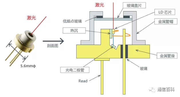
In the figure above, the laser (photodiode) is mounted on a heat sink, connected to electrical pins through gold wires. On top of it, a metal cap and a glass cover sealing window for the laser to pass through are packaged. The cost of TO-CAN packaging is relatively low, but it is difficult to carry larger heat-dissipating devices, and it is generally used in FTTH and wireless access fronthaul scenarios. Butterfly Packaging
As the name suggests, its packaging form resembles a butterfly. It is mainly to solve the heat dissipation problem, providing a larger heat sink, and can also be equipped with a TEC temperature control module, with ceramic submount, chip, thermistor, backlight monitoring, etc. inside. Therefore, a butterfly-packaged device is actually equivalent to an OSA, a device one level higher than TO-CAN.
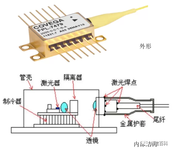
Butterfly packaging has a special packaging form called BOX packaging, which integrates multiple lasers in one packaging space, mainly for multi-channel parallel requirements. Optical transceivers at 25G and below mostly use single-channel TO or butterfly packaging, while those at 40G and above mostly use multi-channel packaging design. Due to the improvement of temperature control facilities in equipment room environments, and with the large-scale use of optical transceivers in the DC data center market, the requirements for cost are getting higher and higher. The hermetic packaging mentioned above requires metal and other supporting materials to build strict protection for fragile optical chips, and the cost is relatively high. Therefore, non-hermetic packaging has been developed in equipment room environments with better temperature control to save cost. Below we briefly introduce non-hermetic COB packaging. COB PackagingSimply understood, it is attaching the laser chip to the PCB substrate, integrating laser arrays and receiver arrays into a small space to achieve miniaturization. Because some protective measures and a large number of auxiliary parts are reduced, the cost is much lower.
In terms of optical chips, let’s first look at the laser at the transmitter end.
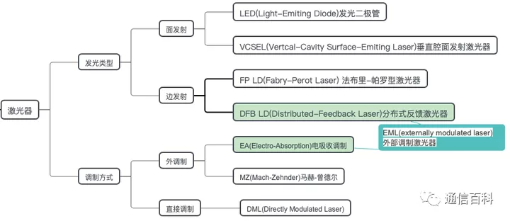
Below we briefly look at several of the most commonly used laser emission devices in optical fiber communication. LED and VCSEL vertical-cavity surface-emitting lasers emit light from the surface, with only different resonant cavity structures. The emission angle of a VCSEL laser is smaller than that of an LED, but larger than that of the later FP/DFB-LD, and it is the lowest-cost chip type, generally used with relatively coarse multimode fiber.
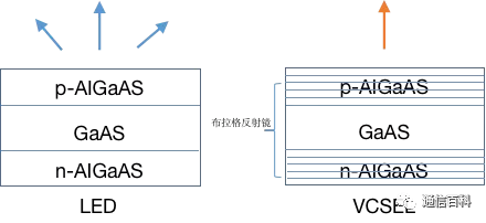
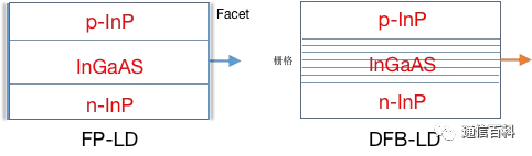
FP-LD and DFB-LD laser diodes are also commonly used semiconductor optical emission devices. They both emit light from the edge, with different resonant cavity structures. DFB is made by processing a grating on the basis of the FP laser to achieve more precise wavelength selection, hence its higher wavelength accuracy.
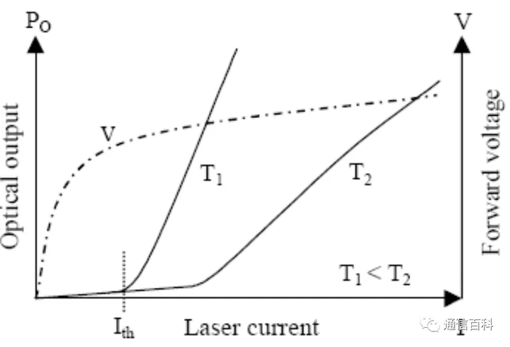
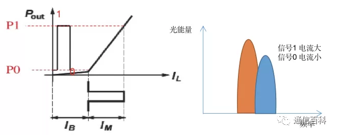
The LD (Laser Diode) here is an electro-optical device. It emits light when the forward current through it exceeds the threshold current (Ith). Therefore, to make the LD operate at high-speed switching, a DC bias current IBIAS greater than the threshold current must be applied.
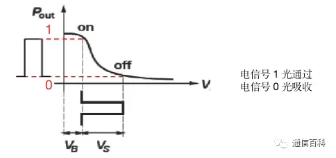
The EML (externally modulated laser) has a different modulation method from the lasers above, which we will discuss in detail below. It consists of one emission chip (such as a DFB) + an external absorption modulator (EA).
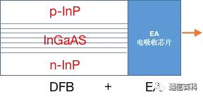
The EML laser is always in the emitting state, and controls the signal output of the laser by controlling the switching of the electro-absorption chip (transparent and opaque). Because the EML laser can be in a relatively stable operating state, the emitted light is also relatively pure, so it is more suitable for long-distance transmission. However, its cost is much more expensive than the DFB above.According to the mind map above, we know that the modulation methods of optical transceivers are two: direct modulation and external modulation. Among them, external modulation lasers have two main modulation methods: EA modulation and MZ modulation.The DFP-LD above is a typical directly modulated laser, that is, it directly uses the “1” and “0” of the electrical signal to control the current magnitude of the laser. A small current means the electrical signal is “0”, which saves energy.
In external modulation, EA modulation also uses the electrical signal “1” and “0” to act on the electro-absorption modulator to control the magnitude of the output light. Its laser is always in the emitting state.
The laser of MZ modulation in external modulation is also always emitting. However, it uses light passing through a Y-shaped waveguide splitter to split into two beams of optical signals with equal and identical phase, and controls the electrodes of the two interference arms through the electrical signal, so that the two beams produce different phases, and then passes through a Y-shaped combiner.
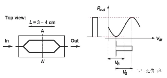
Its effect is: when the signal is “1”, the phases are the same and they superimpose; when the signal is “0”, the phase difference is 180 degrees, and the optical signals cancel out. Besides the lasers above, there is also a “tunable narrow-linewidth laser”, which is frequently used in DWDM dense wavelength division transmission networks. This laser chip can control the output of different wavelengths through current, temperature, and mechanical means. This also makes its structure relatively complex, arguably the most expensive type of laser. I found that the content is too much to finish writing (learning) in one article, so I will continue later. Below is a brief summary to wrap up:
- LED/VCSEL lasers are suitable for short-distance scenarios: about 100 m;
- FP/DFB lasers are suitable for medium-distance transmission: 500 m to 2 km;
- EML lasers are generally used in medium- and long-distance scenarios: 10 km, 20 km, 40 km, 80 km;
- Tunable narrow-linewidth lasers are used in backbone ultra-long-distance, generally wavelength division transmission: greater than 80 km.
Related Reading
- Analysis of 8x100G Technology in the SR Scenario of MSA’s 800G Optical Transceiver
- What Is the 400G DWDM Optical Transceiver Solution Like?
- Optical Transceivers (1): Definition and Composition
Enjoy this article?
Subscribe to get new optical communication insights delivered to your inbox. Free, unsubscribe anytime.