An optical transceiver module consists of three main parts: the optoelectronic devices (TOSA/ROSA), the printed circuit board with electronic components mounted on it (PCBA), and the optical interfaces such as LC, SC, and MPO (the housing).

Transmitter Section
The transmitter section consists of three parts: the light source, the driver circuit, and the control circuit (such as APC). Its main parameters to test are optical power and extinction ratio.

Receiver Section
Taking a PIN as an example, the receiver section is composed of a PIN-TIA (an InGaAs PIN and a transimpedance amplifier) and a limiting amplifier. The incoming optical signal is converted into a photocurrent by the PIN diode, and the photocurrent is then converted into a voltage signal by the transimpedance amplifier. The voltage signal is amplified by the limiting amplifier, and through a shaping filter and the limiting amplifier, differential DATA and DATA-bar signals are produced as AC outputs. It also has a loss-of-signal alarm function: when the optical power is insufficient to keep the module operating normally, the SD pin outputs a logic-low signal to raise an alarm.

Packaging
What Are the Standards and Packaging Form Factors for Optical Transceivers?The basic structure of optical transceiver packaging consists of the transmitter-side module (TOSA) and its driver circuit, and the receiver-side module (ROSA) and its receiver circuit. The technical barriers in TOSA and ROSA lie mainly in two aspects: the optical chip and the packaging technology.
Generally, a ROSA packages an optical splitter, a photodiode (which converts the optical signal into a voltage), and a transimpedance amplifier (which amplifies the voltage signal); a TOSA packages a laser driver, a laser, and a multiplexer. There are mainly the following four packaging processes for TOSA and ROSA:
TO-CAN Coaxial Packaging
TO-CAN coaxial packaging: the housing is usually cylindrical. Because of its small size, it is hard to build in a cooler, and heat dissipation is difficult, making it hard to use for high-power output at large currents, and thus hard to use for long-distance transmission. At present its main applications are still 2.5 Gbit/s and 10 Gbit/s short-distance transmission. But it is low-cost and the process is simple.

TO-CAN Coaxial Packaging
A 10G SFP+ AOC product made with the TO-CAN coaxial packaging process (exploded view)
Butterfly Packaging
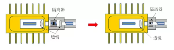
Butterfly packaging: the housing is usually a rectangular box, and the structure and functions are generally more complex. It can house a cooler, a heat sink, a ceramic submount, the chip, a thermistor, and backlight monitoring, and it can support wire bonding for all of these components. The housing area is large and heat dissipation is good, so it can be used for various rates and for long-distance transmission up to 80 km.

Butterfly Packaging
BOX Packaging
BOX packaging is a type of butterfly packaging, used for multi-channel parallel packaging.

BOX Packaging


A 100G QSFP28 LR4 optical transceiver made with the BOX packaging process
COB (Chip On Board) Packaging
COB packaging means chip-on-board packaging, where the laser chip is attached to the PCB substrate. It can achieve miniaturization, light weight, high reliability, and low cost.
For COB packaging, conventional single-channel 10 Gb/s or 25 Gb/s optical transceivers use SFP packaging, soldering the electrical chip and the TO-packaged optical transceiver components onto the PCB to form the module. For a 100 Gb/s optical transceiver using 25 Gb/s chips, four groups of components are needed; if SFP packaging were used, four times the space would be required. COB packaging can integrate the TIA/LA chips, the laser array, and the receiver array into a small space to achieve miniaturization. The technical difficulty lies in the placement accuracy of the optical chip (which affects the optical coupling) and the wire-bonding quality (which affects signal quality and the bit error rate).

A 10G SFP+ AOC product made with the COB process (exploded view)
Summary
Optical transceivers at 25G and below mostly use single-channel TO or butterfly packaging, with standard processes and automated equipment and low technical barriers. But for high-speed optical transceivers at 40G and above, limited by the laser rate (mostly 25G), they are mainly realized through multi-channel parallelism, such as 40G realized by 4×10G and 100G by 4×25G. The packaging of high-speed optical transceivers places higher demands on parallel optics design, high-rate electromagnetic interference, size reduction, and heat dissipation under increased power consumption.
The following optical transceiver device documents can be obtained by scanning the QR code to join ZhiShi XingQiu (Knowledge Planet)!
- Optical Transceiver Handbook.pdf
- Optical Signal Conditioning for Coherent Module Testing.pdf
- Optical Transceivers and Optical Patch Cords Explained .docx
- Fundamentals of Optical Transceivers and Optical Fibers.pptx
- Optical Transceiver Fundamentals Training.ppt
- Introduction to 40G-100G Interface Optical Transceivers.pptx
- The Optical Transceiver and Silicon Photonics Industry from a Customer’s Perspective.pdf
- PON Market Analysis and Optical Transceiver Market and Product Analysis.ppt
- Optical Devices and Optical Transceivers .pdf
- Optical Transceiver Fundamentals Training.pdf
- OpenZR+-400G Digital Coherent Optical Transceiver.docx
- Fundamentals of Optical Transceivers.ppt
- 5G Transport Optical Transceiver White Paper.pdf
- Optical Transceiver Fundamentals Learning Material.pptx
- 800G Optical Transceiver Industry Report.pdf
Related Reading
- HGGenuine’s Differential Packaging Optical Transceiver Solution
- ZTE: Innovation in Heat Sink and Coaxial Packaging Structures for Optical Transceivers
- Huawei & HGGenuine: 50G PON Optical Transceiver Packaging Technology
Enjoy this article?
Subscribe to get new optical communication insights delivered to your inbox. Free, unsubscribe anytime.