Electro-optic modulators convert signals from the electrical domain to the optical domain and are at the core of optical communications, terahertz wireless communications, microwave signal processing, and quantum technologies. Next-generation electro-optic modulators require high-density integration, compact size, large bandwidth, and low power consumption. Existing integrated Mach-Zehnder interferometer (MZI) or microring devices find it difficult to meet these requirements.
Owing to the unique properties of topological photonics, including tight optical confinement, robust light transport, and immunity to defects, integrated lithium niobate (LN) waveguides with topological interface states help address the challenges of next-generation electro-optic modulators.
Topological phase transitions have been used to demonstrate integrated photonic devices, including nonlinear and quantum devices, but the response time of topological devices has been limited to the microsecond scale, and high-speed topological modulators have not yet been exploited.
However, in a paper recently published in Light: Science & Applications, a team of scientists from Shanghai Jiao Tong University and their co-authors developed an ultra-compact, high-speed, large-bandwidth, and energy-efficient electro-optic modulator on a silicon-nitride-loaded lithium-niobate-on-insulator (SiN-LN) platform, featuring topological interface states in a 1D microstructured lattice. Compared with conventional 1D Bragg grating structures, the 1D topological cavity has a shorter length.

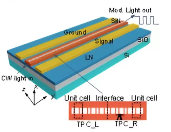
3D view of the modulator based on topological interface states. The inset shows the 1D topological lattice waveguide based on the hybrid SiN-LN platform.
Unlike photonic crystal nanobeam cavities with multiple resonant modes, topological cavities can flexibly control the Q factor and mode volume while strictly maintaining single-mode operation and avoiding mode-number control.

Measured electro-optic S response at different detuning points.
The topological modulator is based on topological interface states, which follow the classic Su-Schrieffer-Heeger (SSH) model and form between two topological photonic crystals in a 1D lattice that have different topological invariants and surface impedances. To obtain a topological interface state at a photonic bandgap, the gap topological invariants of the left and right topological photonic crystals must guarantee a phase difference of π.
A method that spans the topological transition point is used to change the sign of the topological invariant. The device demonstrates excellent performance in ultra-small size, high speed, and high energy efficiency. The topological modulator is described as follows:
The interface state realizes the first topological modulator with a size of only 1.6 × 140 μm², the most compact thin-film LN modulator with a bandwidth exceeding 20 GHz. The peak enhancement of the topological cavity’s electro-optic response is used to break the photon-lifetime-limited bandwidth, achieving a large bandwidth of 104 GHz.
Meanwhile, owing to the small electro-optic mode volume and short electrode length, low RF loss and small capacitance are achieved, yielding an ultra-low energy consumption of 5.4 fJ/bit.
In addition, the demonstrated device can generate 100 Gb/s non-return-to-zero (NRZ) and 100 Gb/s four-level pulse-amplitude-modulation (PAM4) signals.

Measured eye diagram of the PAM4 signal at a data rate of 100 Gb/s.
Related Reading
- How Much Bandwidth Gain Does Increasing the Modulation Order Add?
- 400G+ Optical Transmission Systems: Baud Rate, Modulation, and Spectrum Technologies
- 5G NR Modulation and Coding Schemes – Modulation and Code Rate
Enjoy this article?
Subscribe to get new optical communication insights delivered to your inbox. Free, unsubscribe anytime.