Advanced packaging is a concept derived in response to advanced wafer processes, generally referring to packaging technology that integrates different systems into the same package to achieve higher system efficiency. In other words, as long as a packaging technology can improve the overall performance of the chip (including transmission speed, computing speed, etc.), it can be regarded as advanced packaging. The corresponding traditional packaging, in contrast, packages each chip individually and then assembles these individually packaged chips onto a PCB motherboard to form a complete system, with electrical signal interconnections formed through the PCB.
In industry, face-up chip packaging is generally classified as traditional packaging, where chips are connected to each other (chips to PCB) through gold bonding wires. Advanced packaging, in contrast, generally refers to the flip-chip form, where chips are interconnected with each other (chips to PCB) through solder balls.
Generally speaking, the longer the information transmission distance between chips, the slower the information transfer and the lower the performance of the chipset system. Therefore, at the same chip level, advanced packaging has a shorter transmission distance, corresponding to stronger system performance. Advanced packaging can be roughly divided into two major categories, namely Flip Chip and Wafer Level Package (WLP).

In recent years, based on these two major packaging forms, various specific packaging processes have been derived, including FCBGA, FCLGA, 2.5D/3D packaging, Fan-out, FCCSP, and so on. Although many advanced packaging technologies differ only slightly, due to the customization needs of customers in different application fields, a large number of different types of advanced packaging have emerged in the industry.
From the perspective of downstream applications, application scenarios such as servers, AI chips, PCs, switches, and high-power mining machines that require high transmission rates mostly adopt Flip Chip packaging processes, while smartphones, WiFi, RF chips, power management chips, and low-power mining machines usually adopt WLP packaging processes. For low-transmission, low-computing application scenarios such as flash memory and discrete devices, only traditional packaging in the form of wire bonding, pins (QFN/QFP/SOP), or lead frames is needed.
Typical advanced packaging forms, such as the commonly used packaging for high-performance chips: FCBGA
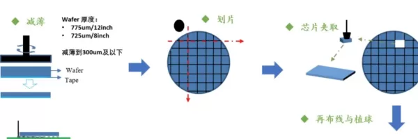
Flip chip, as a typical process of advanced packaging, plays an important role in high-end packaging forms such as FCBGA, CoWoS, and 3D packaging. FCBGA, as one of the simplest flip-chip packaging processes, helps in understanding higher-end CoWoS packaging. The FCBGA packaging process can be roughly divided into the following parts:

(1) Wafer backside thinning: After the wafer is sent from the fab to the packaging house, the first step is to reduce its thickness using a grinding and thinning machine. In the wafer fabrication process, the wafer thickness is generally at the millimeter level and needs to be thinned to below 300um to facilitate subsequent dicing. Downward pressure must be applied during thinning, and the front side of the wafer needs to be protected with UV film to prevent damage to the front-side transistors.
(2) Wafer dicing: The wafer can be cut and diced by laser or mechanical means. At this time, a layer of UV dicing film also needs to be applied to the front side to prevent chip damage caused by excessive cutting-edge stress.
(3) Redistribution layer (RDL) and ball placement: A single die is taken out, and RDL processing is performed on the front side. Through processes such as lithography, etching, film deposition, and cleaning, a multi-layer structure is fabricated to achieve the purpose of chip circuit redistribution. Solder balls are then placed on the corresponding pads and fixed after heating.
(4) Chip bonding: The die bonder fixes the chip to the substrate through thermocompression bonding (TCB), and then removes excess flux and other reagents.
(5) Underfill: After chip bonding, there are air gaps between the solder balls. Since the chip and substrate have different coefficients of thermal expansion, the chip heats up during operation, causing the chip and substrate to expand to different degrees, which in turn pulls on the solder balls and may break them, affecting normal chip operation. Therefore, liquid underfill is dropped on the edge of the chip, and under capillary action it automatically flows into the gaps between the chips, protecting the solder balls after heat curing.
(6) Thermal interface material (TIM) and adhesive application: A layer of TIM adhesive is applied to the back of the chip to enhance heat dissipation, while an adhesive layer is applied around the substrate to facilitate subsequent bonding of the heat spreader lid.
(7) Heat spreader lid bonding: The metal heat spreader lid is attached to the chip, and after baking and heating, the adhesive is cured.
(8) Laser marking: Marking is performed on the surface of the metal heat spreader lid by laser, completing the entire FCBGA packaging process.
Another high-efficiency packaging form: Fan-out
Unlike FCBGA packaging, which dices first and then bonds, wafer-level packaging completes the entire wafer packaging process first and then dices, greatly improving overall efficiency. Wafer-level packaging is mainly divided into two categories: Fan-in and Fan-out. Traditional WLP packaging mostly uses the Fan-in form, applied to ICs with low pin counts, where the overall package area does not increase much compared to the bare die area and the cost is relatively low. In contrast to Fan-in, Fan-out occupies an important position by virtue of its advantages such as low cost, high density, and thin-and-light form. From the perspective of subtypes, Fan-out can be divided into Mold first and RDL first, where the former first molds the chip and then performs wiring and ball placement, while the latter performs wiring first and then packaging.

Taking the Mold first type as an example, the entire Fan-out packaging process is divided into the following parts: first, a thermal release tape is attached to a carrier wafer, and then the KGD (known good die) is picked up and placed on the carrier. Next, a molding machine is used to let epoxy molding compound wrap the entire chip, and then the temporary substrate is removed. Finally, the RDL process is performed at the bottom of the chip, and solder balls are placed. After the packaging is complete, wafer dicing is performed to obtain the finished chips.
The breakthrough solution under limited advanced process: Chiplet
What is a Chiplet? Chiplet means “small chip”, referring to disassembling an originally “large” chip (die) into several “small” chips (dies) at the wafer end. Because each disassembled “small” chip is functionally incomplete, packaging is needed to reassemble the “small” chips and restore the function of the original “large” chip. Chiplet can disassemble a large chip into several small chips with the same process, or into several small chips with different processes.

It is not a specific packaging process, but rather a packaging philosophy. Strictly speaking, Chiplet does not represent a specific packaging form or process, but embodies an approach to advanced packaging. Besides the “homogeneous” Chiplet that cuts a large chip into multiple small chips and then packages them back to achieve functional completeness, there is also the “heterogeneous” Chiplet that packages different types of chips onto one substrate. Through the Chiplet packaging approach, it is possible to:
(1) When advanced process is not available, maintain product performance through chip stacking (advanced packaging/Chiplet) and computing architecture reconstruction. (2) Release domestic advanced process capacity, helping to make up for the scarcity of the process.
Therefore, based on the Chiplet packaging approach, combined with the aforementioned two basic packaging processes of FCBGA and Fan-out, many higher-density packaging processes such as CoWoS, InFO, SoIC, EMIB, and Foveros have been realized.

Related Reading
- Several Advanced Packaging Technologies
- Comparison of the Three Giants’ Advanced Packaging Technologies!
- CPO and 2.5D/3D Advanced Packaging
Enjoy this article?
Subscribe to get new optical communication insights delivered to your inbox. Free, unsubscribe anytime.