What is photolithography?
Photolithography is one of the important processes in the production of integrated circuits (ICs or chips). Simply put, it is the process of replicating circuit patterns onto a substrate using a photomask and photoresist.
The silicon wafer is coated with a silicon dioxide insulating layer and photoresist. Photoresist is easily dissolved by a developer under ultraviolet light irradiation; after dissolution and etching, the circuit pattern remains on the substrate.
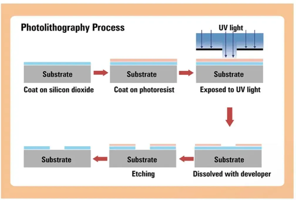
Photoresist is combined with resin, solvent, and additives. The photosensitive range of photoresist is 200 nm to 500 nm. Therefore, many semiconductor laboratories use yellow light to block the 500 nm ultraviolet wavelength, to prevent the photoresist from being overexposed or prematurely exposed.
Why use yellow light?
Because yellow light has a relatively long wavelength, which makes it difficult to expose the photoresist, yellow light is therefore used as the illumination source for the photolithography area.
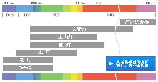
In addition to the above reasons, there are the following points:
- Avoiding interference with the photolithography process
In the semiconductor lithography process, the actual light source used is not yellow light, but deep ultraviolet (DUV) or extreme ultraviolet (EUV) light. These short-wavelength light sources are used to precisely etch fine circuit patterns onto the photoresist on the surface of the silicon wafer.
- Protecting sensitive materials
Certain materials used in the semiconductor production process may be sensitive to certain wavelengths in the visible spectrum, especially to ultraviolet light. Yellow light has a longer wavelength and is less likely to trigger chemical reactions in these sensitive materials.
- Visual comfort
Compared with short-wavelength light such as blue light, yellow light is gentler on the human eye, helping to reduce the visual fatigue of employees working long hours in cleanrooms under high-intensity illumination.
Related Reading
- 2024 Semiconductor Industry Research Report – Automotive-Grade Chips
- 2024 Global and Taiwan Semiconductor Industry Outlook
- What is a Wide-Bandgap Semiconductor?
Enjoy this article?
Subscribe to get new optical communication insights delivered to your inbox. Free, unsubscribe anytime.