What Is Etching
In the wonderful world of semiconductor manufacturing, there is a technology that, like an invisible hero, silently and precisely transfers the fine patterns on the photoresist onto the underlying material — it is etching technology. This technology, like a skilled sculptor, uses a physical or chemical “carving knife” to carve ever-changing patterns on the surface of the silicon wafer.
Imagine that the photoresist layer carries the designed circuit patterns, like jade waiting to be carved, awaiting the fine processing of etching technology.

Figure – Substrate before etching
Etching technology is the “artist” that can precisely replicate these patterns onto the underlying thin-film material. After its processing, the thin-film layer originally hidden under the photoresist becomes clearly visible, leaving only the parts precisely aligned with the photoresist pattern, while the rest is cleverly removed.

Figure – Thin film after etching
So how does this “artist” work? This involves several core parameters of the etching process, which we list below:
- Etch rate
- Etch factor
- Etch selectivity
- Etch uniformity
- Etch cleanliness
Etch Rate
First, let’s look at the etch rate. It is like the sculptor’s hand speed — too fast may result in rough patterns, too slow affects efficiency. The etch rate is usually proportional to the concentration of the etchant. Factors such as the surface geometry of the silicon wafer can affect the etch rate between wafers. Etching a large area of the wafer surface depletes the etchant concentration and slows the etch rate; if the etched area is small, the etching will be faster.

By measuring the film thickness before and after etching, and dividing the difference by the etch time, the etch rate can be calculated:
Etch rate = (thickness before etching – thickness after etching) / etch time
Etch FactorThe etch anisotropy factor determines the directionality of the “carving,” making the etching process more inclined to proceed in the vertical direction, thereby forming steep sidewalls. This parameter characterizes the difference in etch rate in different directions.
Usually a higher etch rate in the vertical direction (depth direction) is desired, forming vertical sidewalls, which is reflected as anisotropic etching. Conversely, if the etching speed is comparable in the vertical and lateral directions, it is called isotropic etching.

The etch factor F is defined as: when etching a line, the ratio of the etched depth V to the lateral increase △X on one side.
F = V/△X
Etch Selectivity
Patterned etching usually involves three materials: the photoresist, the thin film being etched, and the substrate. During the etching process, all three materials are affected by the chemical reaction of the etchant or the ion bombardment in plasma etching. The difference in etch rate between different materials is the so-called selectivity.

Etch selectivity is defined as: the ratio of the etch rate Ef of the material being etched to the etch rate Er of another material such as the photoresist/substrate.
If a target material is etched 10 times faster than the mask or substrate material, then the etch selectivity is 10:1.
Selectivity reflects the “wisdom” of etching technology. It lets the etchant cleverly distinguish which materials need to be removed and which need to be retained, achieving precise removal. This is like a sculptor who can accurately judge which parts need carving and which need to be kept.
Etch Uniformity
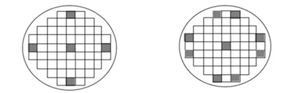
The ideal etching process should guarantee a high degree of uniformity at the wafer level, within the same batch, and between different batches. Etch uniformity is divided into within-wafer uniformity, wafer-to-wafer uniformity, and batch-to-batch uniformity. Uniformity is usually obtained by measuring the thickness at specific points of the wafer before and after etching, such as at the center, edge, and between the edge and center of the wafer, and calculating the etch rate at these points. The points are generally selected by randomly taking 3-5 wafers in a batch, and selecting 5-9 points on each wafer.

Uniformity is very important and must be considered in every step of the chip process, including thin-film deposition, etching, lithography, CMP, and ion implantation. Higher uniformity is needed to guarantee the yield and performance of chips.
Etch Cleanliness
Etch cleanliness is easy to understand. In the etching process, cleanliness must be strictly controlled to ensure that no impurities, polymers, or particulate contaminants remain. Any such contamination may adversely affect subsequent process steps.
Related Downloads:
Lithography and Etching Process.ppt
Integrated Circuit Process: Etching.ppt
Etching Process and Equipment Training.pdf
……..
Related Reading
- New EUV Photoresist
- Do You Know These Properties of Photoresist?
- Why Is Immersion Liquid Used in Lithography Technology?
Enjoy this article?
Subscribe to get new optical communication insights delivered to your inbox. Free, unsubscribe anytime.