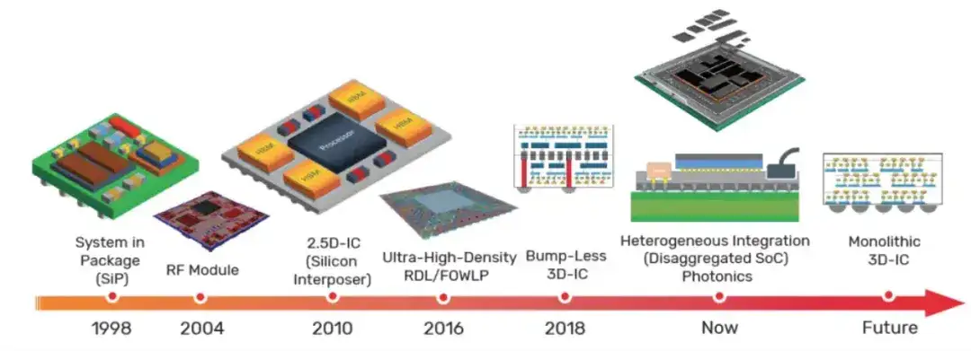
Currently, the vast majority of chip vendors follow the SoC (system-on-chip) path. That is, they purchase soft-core IP or hard-core IP from different IP suppliers, combine them with self-developed modules into a system-on-chip, and then produce the chip at a certain manufacturing process node.
However, in the technology direction beyond Moore’s Law, people generally believe that chiplet technology will be the future direction of chip design. This is a building-block chip-making model that uses internal interconnect technology to package multiple module chips together with a base chip, forming a system chip. As far as we know, a few companies such as Intel have been using chiplet-based technology for several years, but these companies are usually outliers with complete control over the entire design flow.
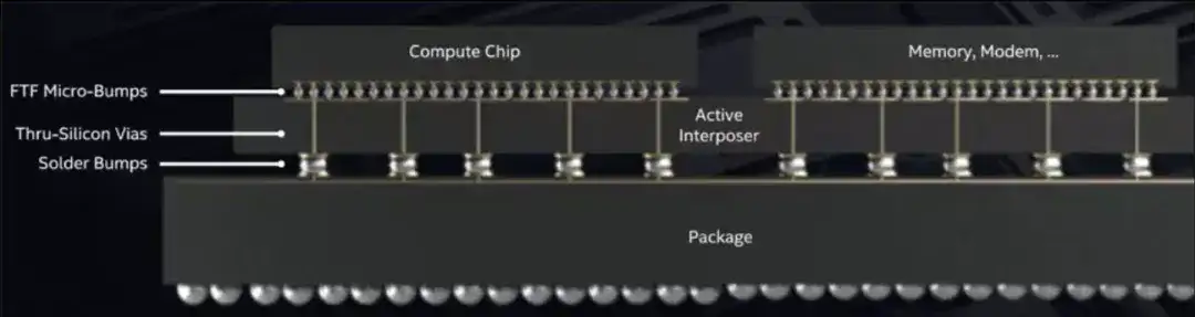
Figure 1: Intel’s Foveros technology for 3D face-to-face chiplet stacking. Source: Internet
And our dream is that, just as today’s system-on-chip designers obtain soft-IP functions from third-party suppliers, we can also obtain hard chip IP from multiple suppliers. It can be predicted that many future chiplets will exceed today’s IC ASICs, ASSPs, and SoCs in size and complexity.
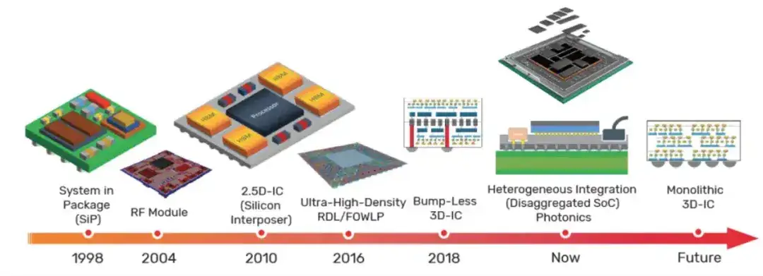
Figure 2: Advanced multi-chip packaging evolution roadmap. Source: Internet
In addition, most of today’s integrated circuits adopt some form of network-on-chip (NoC), which can be regarded as interconnect IP spanning the entire integrated circuit.
So, how will these NoC-based chiplets communicate with each other? That is, how is the “internal interconnect technology” mentioned at the beginning of the article implemented?
For chiplets, a Die-to-Die interface is used, that is, the D2D interconnect scheme of chip-to-chip interconnect/interface technology. This technology directly leverages the characteristics of the extremely short channel connecting the dies, usually consisting of a PHY and a controller module, providing a seamless connection between the internal interconnect structures of the two dies.
There are already multiple Die-to-Die interface schemes to meet such needs. Figure 3 below shows a non-coherent D2D interconnect scheme.
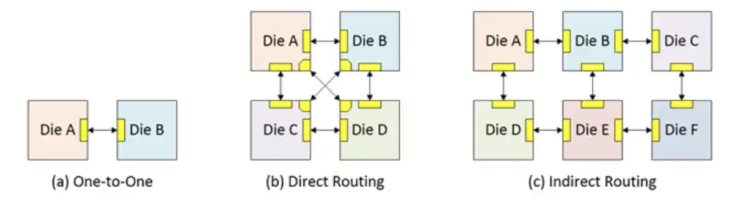
Figure 3: Three examples of non-coherent interconnect. Source: Internet. As shown in Figure 3a above, two chiplets are directly connected via D2D, which is relatively simple. More complex cases involve multiple chips (Figure 3b), still with direct D2D connection and static mapping-mode configuration at startup. In the case of indirect D2D routing involving chiplet hopping (Figure 3c), there are two possibilities: static mapping-mode configuration at startup or dynamic mapping-mode configuration at runtime.
Of course, we can also consider using coherent D2D interconnect, as shown in Figure 4. In this case, in addition to the memory on any chiplet such as processor and accelerator caches, we also show the possible deployment of external memory (MEM) such as DDR, the larger gray rectangle. These memories are the external memory of the multi-chip system package and require memory-controller IP on the chiplet, as shown by the smaller gray rectangle.
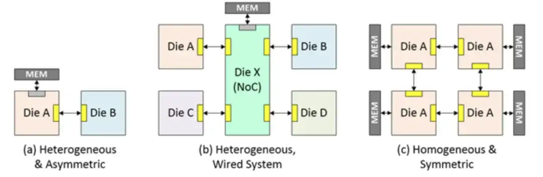
Figure 4: The figure above shows three examples of coherent interconnect. Source: Internet
The simplest form of coherent interconnect is heterogeneous and asymmetric, as shown in Figure 4a. In this case, there is a clear host chiplet connected to external memory. Figure 4C is the interconnect of a homogeneous symmetric architecture, in which each chiplet can talk to its own memory and to the memory of all other chips.
Let us continue to take a deeper look at the D2D interconnect scheme, as shown in Figure 5. We will start with the NoC adopted by the chiplet itself. Designers can use various NoC technologies.
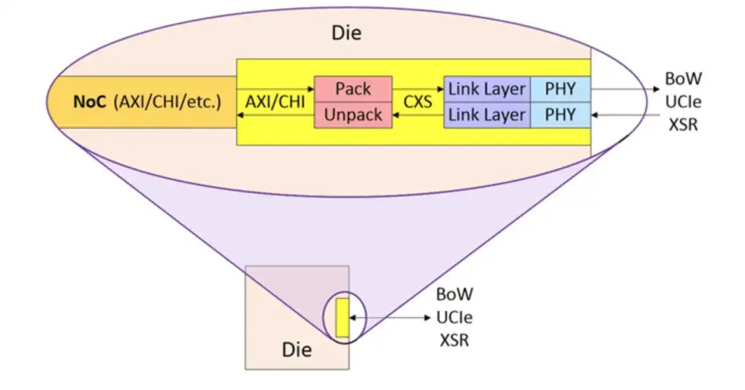
Figure 5: D2D interconnect example highlighting the NoC (left)
For example, Arm’s Advanced Microcontroller Bus Architecture (AMBA) adopts the non-coherent Advanced eXtensible Interface (AXI) protocol and the Coherent Hub Interface (CHI) protocol. Assuming our designers use NoC protocols such as AXI or CHI, or the NoC IP can generate and receive AXI or CHI traffic, then any outbound traffic must be packaged into a streaming-interface format such as CXS.
The physical layer will be implemented using technologies such as Bunch of Wires (BoW), Universal Chiplet Interconnect Express (UCIe), or Synopsys eXtra Short Reach (XSR). Similarly, inbound traffic will pass through the associated PHY and link layer and be decompressed into AXI or CHI.
Finally, it should be noted that chiplet technology is still in the exploratory stage, but regardless of the details, because of its numerous advantages in cost, yield, flexibility, scalability, and customization, chiplets and multi-chip systems will be the future trend of electronic design!
Related Reading
- How Did the Packaging and Multiplexing Path from OTN to Flexible FlexO Evolve?
- What Packaging Processes Are There for Optical Modules?
- Several Advanced Packaging Technologies
Enjoy this article?
Subscribe to get new optical communication insights delivered to your inbox. Free, unsubscribe anytime.