In the previous issue we discussed Fiber Bragg Grating, which, together with a circulator or other isolation components, can realize multiplexing and demultiplexing. //What Is a Fiber Bragg Grating?//
Today let’s look at another commonly used multiplexing/demultiplexing device: the Arrayed Waveguide Grating, abbreviated as AWG.
But before talking about AWG, let’s first take a look at what planar lightwave circuit (PLC) technology is.
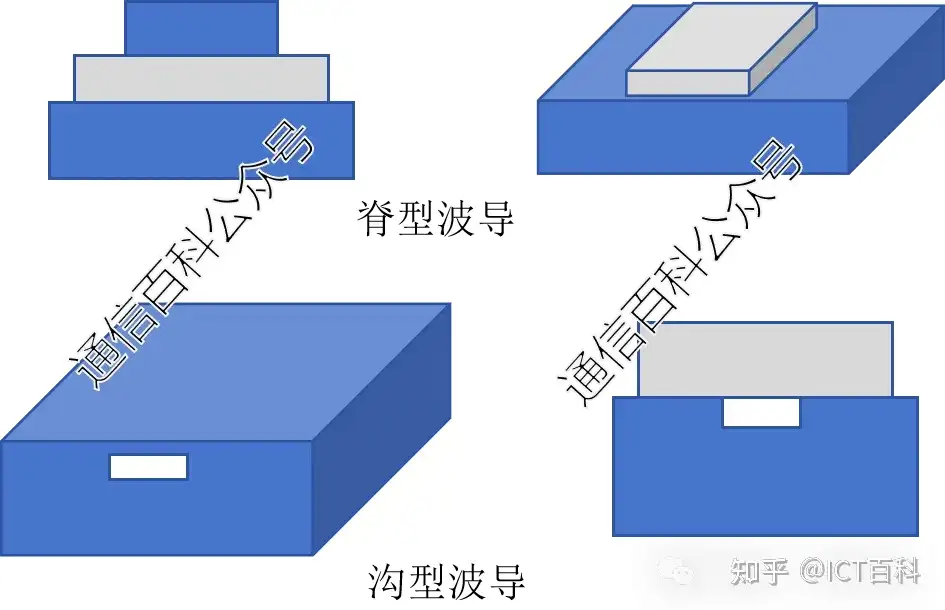
A waveguide is a medium used to confine light waves. Why is confinement needed? The purpose is to effectively restrict the propagation of light waves in a specified direction or space. For example, optical fiber can confine light to propagate within the core layer. Optical fiber is a kind of waveguide, a circular optical waveguide. Or there are rectangular waveguides, planar waveguides, etc.
As shown below is a rectangular waveguide, also called a strip waveguide.
Related to today’s AWG is the planar optical waveguide, which can be made of thin films, usually composed of at least three layers of thin-film materials with different refractive indices, so it is also called a thin-film waveguide. Usually, the refractive index of the waveguide layer (core layer) is larger than that of the upper and lower cladding layers.
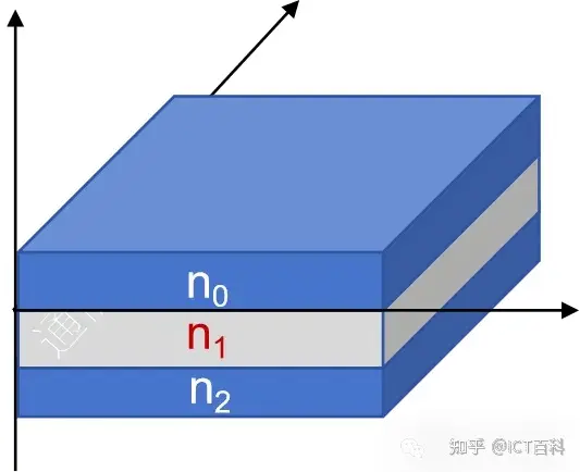
When a light beam enters the waveguide from one side at an appropriate angle, due to the difference in refractive index, the light wave repeatedly reflects and advances inside the core layer without scattering sideways, thereby realizing the confinement and directional transmission of the light beam.
Using PLC technology, many things can be done: gratings, splitters, and also optical switches can be made.
Our arrayed waveguide grating AWG is the first component to commercialize PLC technology.
Structurally, an AWG consists of an input optical waveguide, a slab waveguide, a waveguide array, a slab waveguide, and an output waveguide. As shown below:
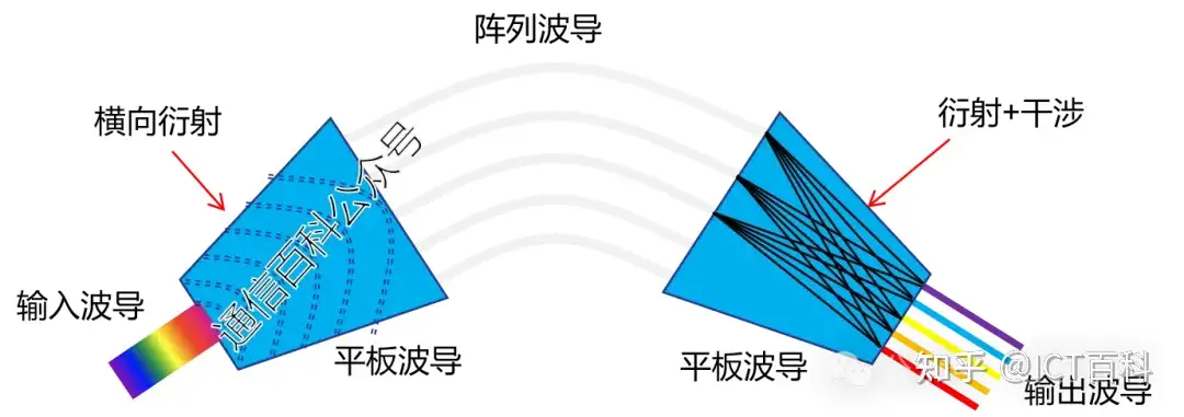
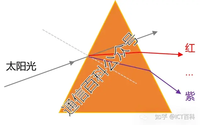
The AWG arrayed waveguide grating schematic looks very complex, but it is actually a kind of optical “splitter.” Simply put, it can separate light of different colors, just like the triangular prism in our junior high school physics class, which can split white light into seven colors.
Back to the AWG, the waveguide units inside it are like transmission pipes of customized lengths. When optical signals propagate in different waveguide units, the diffraction and interference effects of light are used to realize the functions we need.
What is diffraction? Look at the figure below. When light passes through a slit, diffraction occurs, producing alternating bright and dark fringes on both sides of the slit.
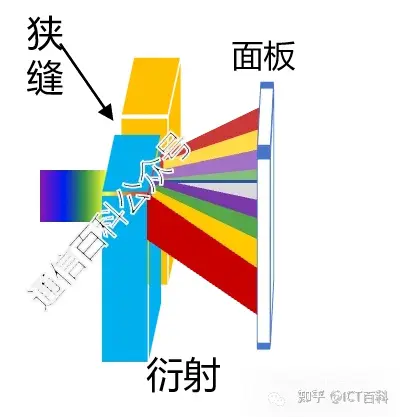
I won’t go into interference in detail. Everyone should know the “terrifying” Young’s double-slit interference experiment. My shallow understanding is that two light waves pass through two slits, each slit produces diffraction, and then the diffracted light waves from the two slits interfere due to the phase difference, making the fringes deeper or shallower. What about multiple slits?
For example, replacing the panel in the figure above with a grating:
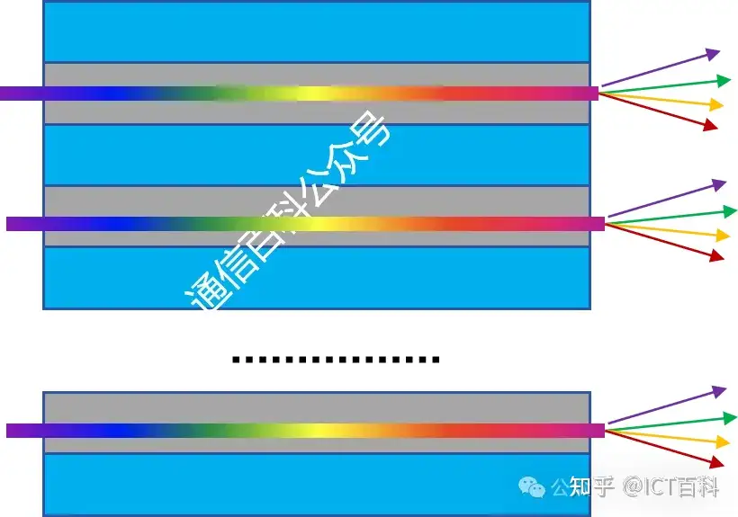
For an AWG, this is exactly how it works: it realizes dispersion and spatial separation of light.
Let’s specifically sort out the process by which an AWG realizes demultiplexing:
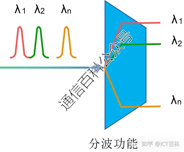
The specific process after light enters the arrayed waveguide grating (AWG) can be described in detail as follows:
- Input optical waveguide
The composite light beam carrying multi-wavelength optical signals enters the AWG through the input optical waveguide. The role of the input optical waveguide is to uniformly introduce the input optical signal into the subsequent optical processing structure.
- First slab waveguide
After passing through the input optical waveguide, the optical signal enters a section of slab waveguide, whose role here is to perform preliminary propagation and distribution of the optical signal to ensure uniformity when it subsequently enters the waveguide array.
- Waveguide array
Subsequently, the optical signal enters the key waveguide array region. The waveguide array consists of a series of waveguides with gradually changing lengths, whose length differences are designed according to the following formula to realize phase adjustment of optical signals at different wavelengths:
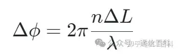
Here, I(x) is the phase difference produced after the light wave passes through the waveguide length difference L, n is the refractive index of the waveguide material, and λ is the wavelength of the light wave. Different wavelengths accumulate specific phase delays in waveguides of different lengths, thus having different phase relationships when leaving the arrayed waveguides.
- Second slab waveguide
The optical signal that has passed through the waveguide array enters another slab waveguide region again. At this time, optical signals of different wavelengths with specific phase differences meet and interfere in the slab waveguide. The interference effect causes the light of specific wavelengths to be enhanced at specific positions, forming interference maxima, while weakening or disappearing at other positions. The intensity distribution of the interference pattern can be understood using the interference formula:

Here I(x) is the light intensity at position x, I1 and I2 are the intensities of the two interfering beams respectively, k is the wavenumber, and x is the spatial position.

is the initial phase difference of the two beams.
As mentioned above, in an AWG, although it is not simple double-slit interference, the interference principle still applies, only the interference occurs among the beams output from multiple waveguides.
- Output waveguide
Finally, the optical signals separated by the interference effect, with each specific wavelength having maximum intensity at a specific position, are output to their respective channels through the output waveguides. Each output waveguide corresponds to a specific wavelength range. Therefore, optical signals of different wavelengths are precisely separated and directed to their respective output ports.
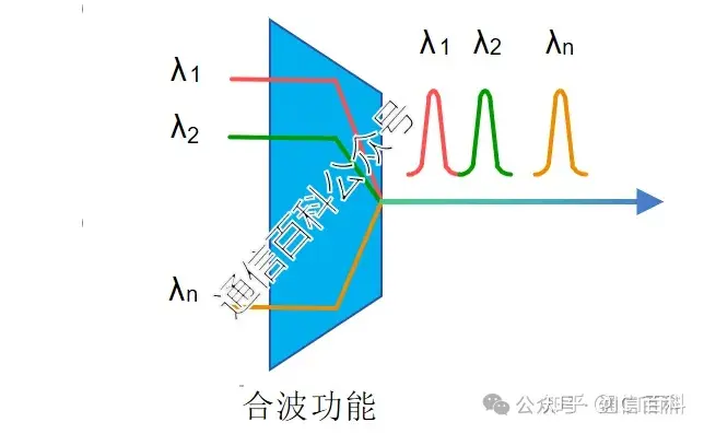
The above describes the demultiplexing function of the AWG. When optical signals are input to the AWG from the opposite direction (reverse), since the physical structural characteristics of the AWG (waveguide lengths and phase relationships) remain unchanged, these optical signals of different wavelengths will be combined at the output end according to the same phase and amplitude relationships, thereby realizing the multiplexing function of optical signals.
Related Reading
- Silicon Photonics Series 1: How to Let Light Enter the Waveguide Smoothly from the Fiber?
- Why Is the TE Mode More Popular Than the TM Mode in Silicon Photonic Waveguides?
- Silicon Photonic Waveguides: How to Ensure Light Polarization at the Receiving End?
Enjoy this article?
Subscribe to get new optical communication insights delivered to your inbox. Free, unsubscribe anytime.