In the semiconductor field, a photomask is equivalent to the “negative” used by old cameras for taking photos. Lithography is performed on this “negative,” accurately transferring the pattern on it to the photoresist below. (Many post-90s and post-00s readers may never have come across this “negative” thing.)
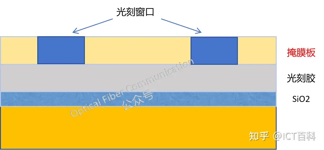
The materials used to make photomasks are mainly composed of a high-quality quartz glass substrate and a light-shielding material deposited on the surface, where the light-shielding material is usually chromium (Cr). Chromium film is chosen because its deposition and etching are relatively easy, and it is completely opaque to light.
So does the photomask need to cover all positions of the photoresist? Actually not. This depends on the required circuit pattern design; light-transmitting and light-blocking regions are arranged alternately, so that only specific photoresist regions are exposed or kept unexposed, and then through subsequent steps such as development and etching, the required circuit pattern is formed on the wafer surface.
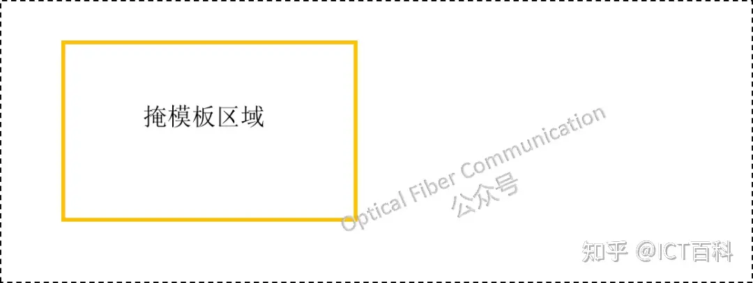
Let me draw a Layout view as an example, which may only be a small portion.
So in the semiconductor manufacturing flow, do we only use a photomask once, or use the mask process only once? The answer is also no. For example, in multi-layer interconnection, it may need to be repeated multiple times; each additional circuit layer requires a new photomask to build a multi-layer complex integrated-circuit structure.
To gain a deeper understanding of photomasks, let us use two steps in the CMOS process as examples and discuss them specifically.
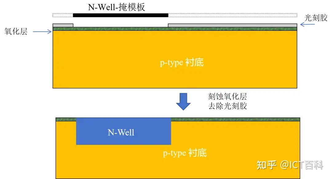
First, look at the N-Well photomask:
In the CMOS process, in the step of forming the N-Well region, the N-Well photomask is used to image the photoresist on the grown oxide layer. This imaging process only exposes the N-well region, laying the foundation for the subsequent etching step. After etching is completed, the photoresist is removed, and n-type impurity diffusion is performed, forming the N-Well in the p-type substrate.
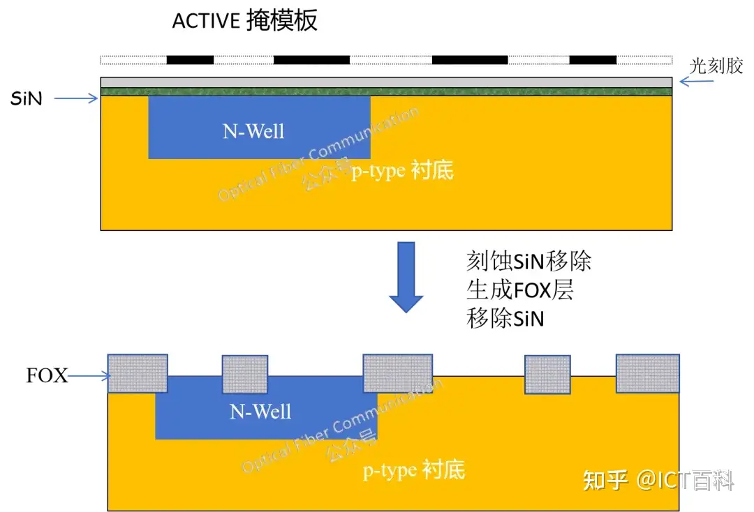
Next, the ACTIVE photomask is used for the fabrication of the active region. In this step, photoresist is first deposited on the SiN layer, and then the ACTIVE photomask is used for photoresist imaging. The imaged SiN layer is removed by etching, providing conditions for growing the field oxide (FOX).
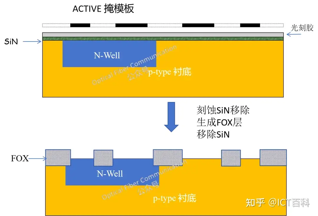
In the above flow, we used the N-Well photomask and the ACTIVE photomask. Subsequent flows also have the POLY photomask for forming the polysilicon gate, the CONTACT photomask for determining the positions of contact holes between the metal layer and the semiconductor or polysilicon, and the VIA photomask for achieving communication between multiple metal layers. We will not go into detail here; when we discuss the CMOS process flow later, we will talk about them in detail.
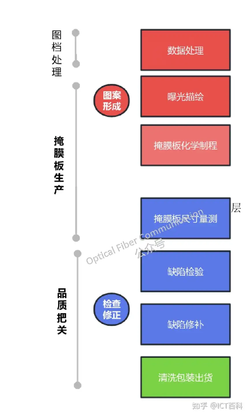
It can be said that the application of photomasks is spread throughout every link of semiconductor manufacturing, from basic transistor construction to advanced multi-layer interconnect systems, everywhere. Therefore, photomask manufacturing is very important and directly related to the yield of semiconductor devices. Nowadays, photomask manufacturing and production are basically outsourced. Below, let me place a diagram so everyone can roughly understand the photomask production flow:
Related Reading:
- What Is a Tungsten Plug (W-Plug)?
- Is Through-Hole Technology Really Useless Compared with SMT Surface Mount Technology?
- How to Form a Uniform Photoresist Film on a Wafer?
- Do You Really Understand Reliability and Burn-In?
- What Is CoWoS Packaging Technology?
Enjoy this article?
Subscribe to get new optical communication insights delivered to your inbox. Free, unsubscribe anytime.