In our article the day before yesterday, “What Exactly Is a Photomask?”, we said that a photomask is like the “negative” of an old camera. In fact, the lithography field also has something similar to our “photographic paper,” namely the “photoresist.” Photoresist is coated onto the wafer and then exposed to light, “printing” the pattern on the negative onto the “photographic paper.”
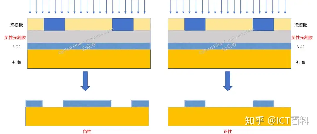
Photoresist has a more formal name, photoresist (abbreviated P.R.). So if you see “resist” in some places, you should know it refers to photoresist. In addition, depending on how it reacts under light-energy-beam irradiation, it is divided into negative photoresist and positive photoresist. What is the difference between positive and negative resists? Simply put, when irradiating the wafer, in the area not blocked by the mask, negative photoresist retains the pattern. Positive photoresist is the opposite: the irradiated area can be removed after development, while the unirradiated area is retained. Let us draw a diagram to understand!
After understanding the basic principle of photoresist, let us look at several key properties of photoresist:
Sensitivity:
The sensitivity of photoresist usually refers to its degree of response to the exposure light source (usually ultraviolet light), that is, how easily the photoresist undergoes a chemical reaction. If the sensitivity is too low, it affects production efficiency, so we usually want the photoresist to have high sensitivity, because a high-sensitivity photoresist can undergo sufficient photochemical reaction at a lower exposure dose, forming the desired pattern during development. However, too high a sensitivity is also bad, because it affects resolution. Speaking of resolution, what is that? Resolution:
The resolution of photoresist refers to the minimum feature size that the photoresist can form in the lithography process, that is, the smallest line width or spacing that can be produced. In an ideal case, lithography resolution can be estimated by the Rayleigh Criterion, which is based on the optical diffraction limit. The formula is as follows: Resolution = 1.22λ / NA, where:
- λ is the wavelength of the exposure light source;
- NA is the numerical aperture, determined by the objective lens of the lithography machine and the illumination conditions.
So what is the relationship between sensitivity and resolution? There is actually a formula for it, but we will not go into detail here. Simply put, the higher the sensitivity, the worse the resolution, and vice versa. For the third property, let us talk about the contrast of photoresist.
Contrast: a more official description: contrast is a parameter describing the photoresist’s response characteristics to light, related to the relationship between the exposure dose and the photoresist’s response. The higher the contrast, the more sensitive the photoresist is to small changes in exposure dose, producing clearer pattern edges. Let me use an analogy to make it more accessible.
- High-contrast photoresist (like a sensitive pen): with a light stroke, this pen leaves a clear line on the paper, suitable for drawing fine patterns. In photoresist terms, this means very small changes in exposure dose can produce obvious differences on the resist, so very fine circuit patterns can be produced.
- Low-contrast photoresist (like an insensitive pen): this pen needs many hard strokes to leave a mark, suitable for drawing thick-line patterns. In photoresist terms, this means larger changes in exposure dose are needed to produce an effect, making it unsuitable for fine circuit patterns.
In addition, the thickness of the photoresist also affects contrast and resolution; thinning the resist film can improve contrast and resolution. In general, the contrast of photoresist ranges from 0.9 to 2.0. Finally, a small question: Typically, between negative and positive photoresists, which has higher or lower sensitivity, resolution, and contrast?
Thank you for reading!
Published with the permission of OFC.
Related Reading
- New EUV Photoresist
- How Are Photoresist Patterns “Copied” onto Chip Material?
- Why Is Immersion Liquid Used in Lithography?
Enjoy this article?
Subscribe to get new optical communication insights delivered to your inbox. Free, unsubscribe anytime.