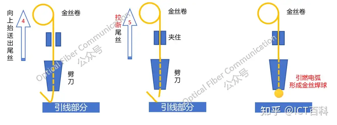
To better understand today’s topic, let us first look at the interface of signal connection inside and outside a semiconductor.
In traditional packaging forms, internal connections still mainly use wire bonding, while external connections usually use lead frames and ball grid arrays. Today we mainly discuss wire bonding for internal connections. Through wire bonding, bare dies are interconnected, thereby enabling more complex functional integration.

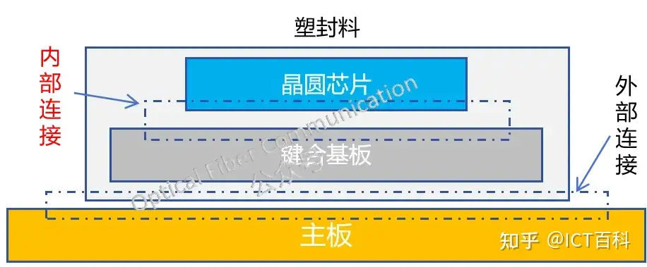
Wire bonding technology is precisely the bridge that realizes this connection. It uses thin metal wires (such as gold, aluminum, or copper) to precisely connect the bonding pads on the chip with the I/O leads inside the package.
In my understanding, this bonding process mainly uses brute force (mechanical pressure) or electric welding (thermal energy). In official terms, it provides energy to break the oxide layer on the bonded surface, bringing the metal wire into close contact with the bonded surface, reaching the range of interatomic attraction and causing atomic diffusion at the interface to form a welded joint, thereby achieving bonding. There are three commonly used wire bonding methods:
- Thermocompression Bonding (TCB): a bonding technique performed at high temperature and pressure, commonly used for gold wire bonding.
- Ultrasonic Bonding (USB): uses the vibration energy generated by ultrasonic waves to achieve the connection between metal wire and bonding pad, usually used for aluminum wire bonding.
- Thermosonic Bonding (TSB): combines thermal energy and ultrasonic energy, suitable for bonding gold and copper wires.
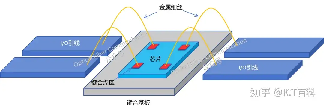
In the TSB bonding process, a spherical solder joint is first formed at one end of the gold wire. This joint is called the gold ball (free-air ball). The device used for bonding is illustrated below:
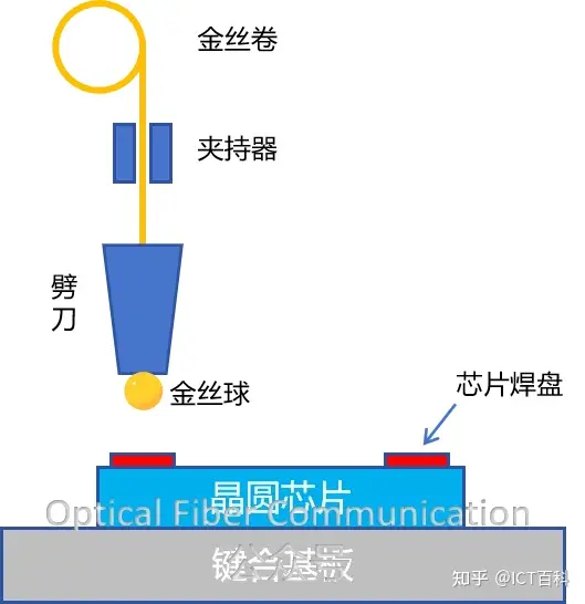
Let us look at the wire bonding process in detail below. First, before bonding, the chip’s bonding pads need to be cleaned to remove the oxide layer and contaminants on the surface, ensuring good contact between the metal wire and the bonding area. This cleaning can be chemical cleaning, plasma cleaning, or mechanical grinding. In some advanced packaging technologies, a layer of metal or alloy may be pre-coated on the pad to improve bonding performance and provide a better bonding interface. After cleaning, we ensure that the pad and the pins on the substrate are aligned. Then the first bonding is performed, forming a flat spherical connection joint under the action of pressure and temperature.
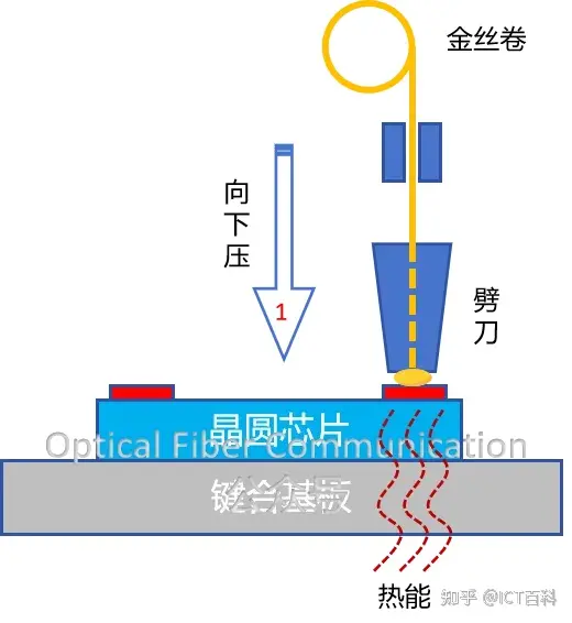
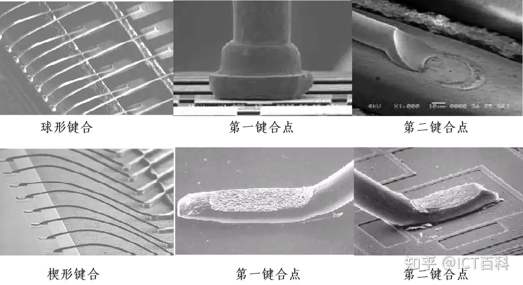
Then the capillary is lifted and moves at high speed to the second bonding point, at which time the gold wire is drawn into an arc-shaped loop. The minimum thickness of the gold wire – I found a figure of about 15 um. Then, under the action of pressure and high temperature, the second connection is formed, and the shape of this joint is a wedge.
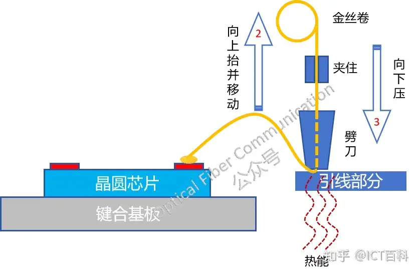
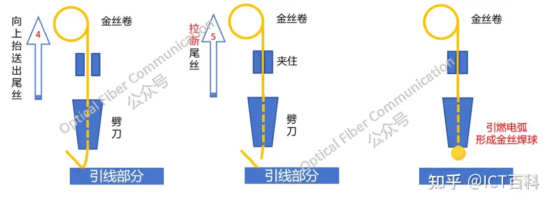
Then the capillary is lifted to a certain height, a little tail wire is fed out and then broken off, and finally an electric arc is struck to form a gold ball, entering the next bonding cycle. Repeating this process forms the interconnection structure shown in the second image above.
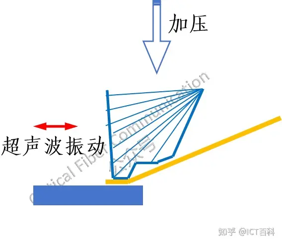
The above can also be done with ultrasonic waves. Under the action of ultrasonic waves, the capillary undergoes horizontal elastic vibration, and under the combined force of pressure, it rapidly rubs against the metal surface of the bonding area, causing plastic deformation. The difference is that both bonding joints are wedge-shaped.
Let us put up two images found online, showing the shapes of the first bonding point and the second bonding point for ball bonding and wedge bonding respectively.
In the past, this work was done manually, but now there are dedicated wire bonding machines that automate it. However, as electronic devices move toward smaller sizes and higher performance, wire bonding technology has begun to face challenges from wire diameter limits and connection density. To overcome these limitations, flip-chip technology was invented. We will discuss flip-chip technology separately later.
Okay, that is all for today. Typing is not easy + drawing is too slow, and it took me most of a day. If there are any inaccuracies, please understand and point them out.
Thanks for reading!
Published with authorization from OFC!
Related Reading
- How Did the Road from OTN to Flexible FlexO Packaging and Multiplexing Unfold?
- What Are the Packaging Processes for Optical Modules?
- Several Advanced Packaging Technologies
Enjoy this article?
Subscribe to get new optical communication insights delivered to your inbox. Free, unsubscribe anytime.