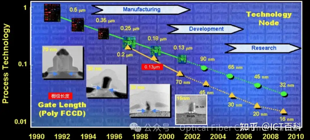
The 0.13μm process, in the semiconductor field, refers to the gate length of the transistor and represents a technology node. We know that the gate length directly affects the switching speed and current driving capability of the transistor, so generally we want the gate to be as short as possible.
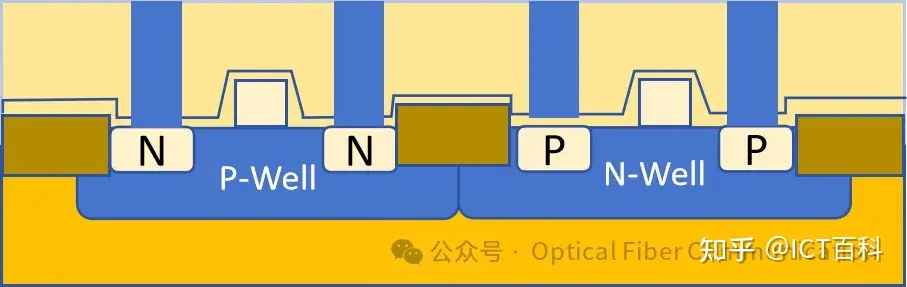
Being short has many benefits, including allowing more circuit elements to be integrated on a silicon wafer of the same area, greatly improving the computing power and performance of the chip. A shorter gate length also means the transistor can operate at higher frequencies while reducing current leakage, thereby improving energy efficiency and running at lower power.
Looking back at the history of semiconductor development, from the first mass production of MOSFETs to the late 1990s, the process node more or less referred to the transistor’s gate length (Lg), which was also considered the “minimum feature size.” For example, Intel’s 0.5 μm process had a gate length of 0.5 μm. This continued until the 0.25 μm process in 1997, when Intel began introducing more aggressive gate-length scaling. For example, their 0.25 μm process had a gate length of 0.20 μm, and likewise their 0.18 μm process had a gate length of 0.13 μm. The figure below shows Intel’s early semiconductor roadmap.
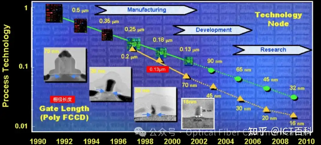
It can be seen that at these nodes, the number describing the “process node” is actually larger than the gate length. The process node is also called the technology node, which describes the semiconductor manufacturing process and its design rules. In the early days, the naming of process nodes was directly related to the transistor’s feature size, such as the gate length.
Especially in recent years, due to marketing strategies and differences among foundries, node names have gradually lost their exact meaning. For example, nodes like 22nm, 16nm, 14nm, and 10nm now represent a specific generation of chips manufactured by a particular technology rather than the specific gate length. For instance, the gate length of the 10nm process node is roughly between 10nm and 20nm.
Of course, Moore’s Law cannot be escaped here. It predicts that the number of transistors on an integrated circuit doubles roughly every two years. To achieve this, the feature size of each new node needs to shrink by a factor of about 0.7. Specifically, to achieve the doubling of density, the contacted poly pitch (CPP) and minimum metal pitch (MMP) need to scale by about 0.7 times per node, which can be expressed as: 0.7x CPP · 0.7x MMP ≈ ½ area.
Although shrinking the gate length can bring performance improvements, after the 45nm process node, gate-length scaling basically stalled. This is because, as dimensions shrink, quantum effects become more significant, causing further gate-length reduction to bring undesirable physical effects such as increased leakage current and unstable transistor performance.
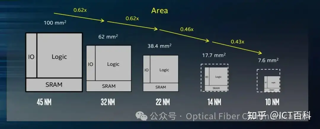
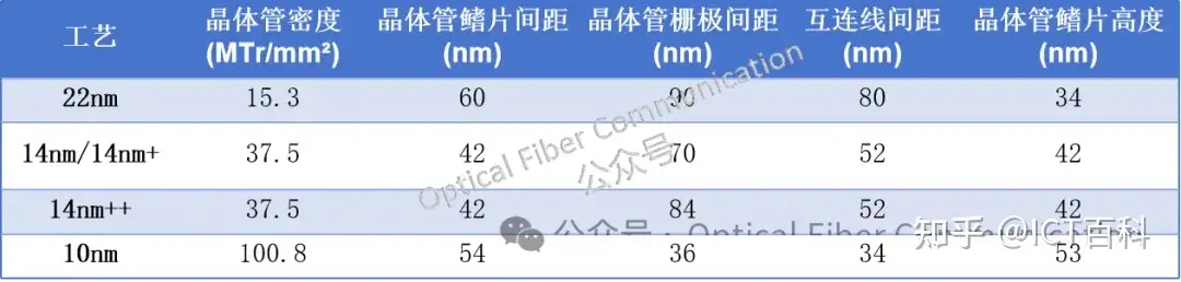
To solve these challenges, Intel introduced fin field-effect transistors (FinFET) in its 22nm process, allowing transistor density to continue increasing while the gate length remained basically unchanged. For example, in Intel’s 14nm FinFET technology, the fin pitch is 42nm and the fin height is 42nm. In the 10nm process, Intel’s fin pitch is 34nm and the fin height is 53nm, meaning the fins are taller.
With the advancement of technology, the concept of half-nodes emerged, also known as “node-let” technology. Half-nodes represent incremental improvements between full process nodes, typically involving 0.9x linear scaling.
For example, in the transition from the 90nm process to the 65nm process, half-node products like 78nm or 70nm may appear. Now, with the full-node processes of 10nm and 7nm and between 5nm and 3nm, half-node technologies such as 12nm, 11nm, 8nm, 6nm, and 4nm have been introduced. Although it is unclear whether all node processes will exist long-term, this node-let technology allows manufacturers to improve chip performance and energy efficiency through some refinements and optimizations without fully entering the next full-node process.
In summary, from the 0.13μm process node to today’s 7nm and 5nm, and possible smaller dimensions in the future, the gate length is no longer the direct basis for process-node naming, but it remains a key parameter for measuring transistor size and performance.
Thank you for reading!
Enjoy this article?
Subscribe to get new optical communication insights delivered to your inbox. Free, unsubscribe anytime.