In the semiconductor photolithography process, when light passes through holes on the mask or passes sharp edges, the light intensity distribution changes direction due to diffraction effects. At the same time, diffraction takes away the exposure energy and causes the light to diverge, exposing areas on the photoresist that should not be exposed.
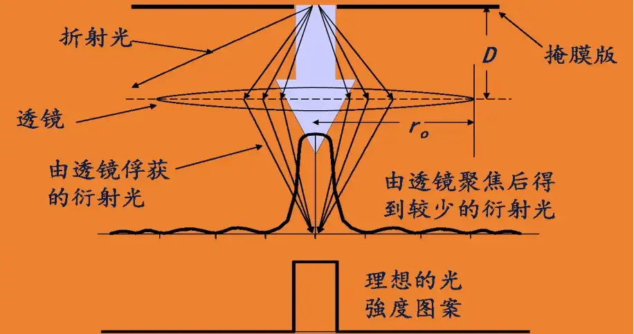
To suppress the impact of diffraction effects on resolution, the optical system needs the ability to efficiently converge diffracted light, which requires a lens. A lens can capture some diffracted light, and we call the lens’s ability to collect diffracted light the numerical aperture (NA) of the lens. The numerical aperture is defined by the following formula:
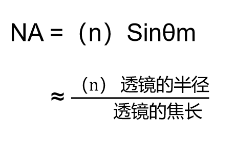
Where n is the refractive index of the medium, and θm is the angle between the principal optical axis and the edge of the lens.
In traditional dry lithography systems, under the inherent limitation of air medium refractive index n=1, the objective lens is usually designed with θm of about 72 degrees, corresponding to a theoretical NA of 0.95; while immersion lithography, under the equivalent optical design concept, introduces a high-refractive-index liquid of n=1.44 and optimizes the lens curvature, extending θm to about 68 degrees, achieving a key leap to NA=1.35.
Related Reading
- New-Type EUV Photoresist
- How Are Photoresist Patterns “Copied” onto Chip Materials?
- Do You Know These Characteristics of Photoresist?
Enjoy this article?
Subscribe to get new optical communication insights delivered to your inbox. Free, unsubscribe anytime.