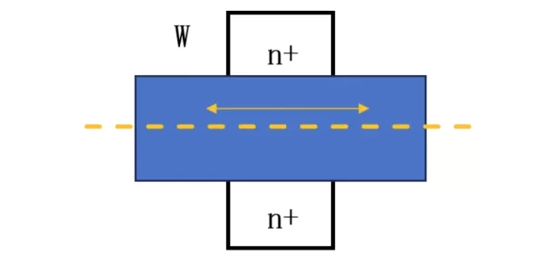
The channel width (usually denoted by W) is the lateral physical dimension of the conductive channel between the source and drain in a metal-oxide-semiconductor field-effect transistor (MOSFET), that is, the width perpendicular to the direction of carrier flow.

When the channel width W shrinks to approach the lateral extension scale of the depletion layer, the threshold voltage V_T will rise significantly as W decreases. This phenomenon is called the narrow-channel effect on threshold voltage. Its physical origin lies in the thick oxide layer of the LOCOS (field oxide isolation) structure restricting the extension of the depletion layer at the channel edge, forcing the gate voltage to additionally compensate the edge barrier to achieve full-channel inversion.

It should be distinguished from the short-channel effect – the latter is caused by the reduction of channel length L, manifesting as V_T decline and drain-induced barrier lowering (DIBL) due to degraded gate control.
PS: The short-channel effect is the gate control failure caused by the scaling down of the longitudinal dimension L, manifesting as V_T decline and leakage runaway; the narrow-channel effect is the edge-field distortion under the reduction of the lateral dimension W, causing an abnormal rise in V_T.
The narrow-channel effect occurs because when the channel width W becomes smaller, the increase in threshold voltage V is mainly caused by charges stored under the field oxide.
It should be noted that the short-channel effect is related to the device isolation method. For field oxide isolation, the narrow-channel effect occurs; for trench-isolated devices, the narrow-channel effect basically does not occur, and the threshold voltage generally does not increase as W becomes smaller.
Enjoy this article?
Subscribe to get new optical communication insights delivered to your inbox. Free, unsubscribe anytime.