The integration level of semiconductor chips is getting higher and the density is getting larger. This directly brings about a change: the number of pin terminals required on the chip also increases substantially.
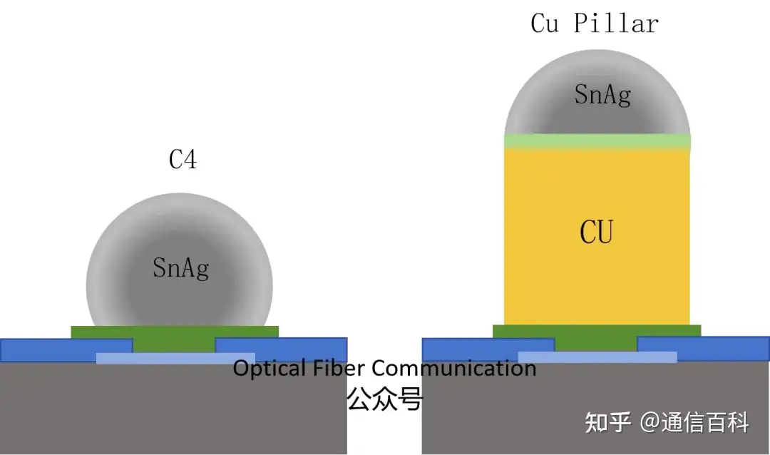
To keep up with this trend while coping with ever-smaller pin pitches, the industry’s mainstream solution is to use Cu Pillar (copper pillar) to replace the traditional C4 solder balls, to realize the interconnect between the chip and the substrate.
In our article yesterday “
HiSilicon’s 7.2T High-Density Hi-ONE Silicon Photonics Engine
It was mentioned that Huawei HiSilicon also uses Cu Pillar technology in its 7.2T Hi-ONE silicon photonics engine.
Let us first talk about what a solder ball is, that is, C4 – not C4 explosives.
The C4 here is fully called Controlled Collapse Chip Connection, translated as “controlled collapse chip connection technology”.
The diameter of a C4 bump is about 75 to 150um. In the C4 process, after reflow melting and re-solidification, its shape is not exactly a perfect sphere, but more like a dome-shaped or mushroom-shaped bump.
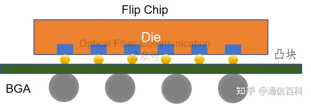
Note: In FC flip-chip packaging, C4 bumps are used to connect the chip to the package substrate, while BGA solder balls are used to connect the package substrate to the external circuit board.
Besides replacing C4 in internal connections, the application range of Cu Pillar is also expanding. Cu Pillar technology is extending from the chip level to the board level. For example, vendors such as ASE and Amkor are promoting the application of Cu Pillar in FC-BGA.
So what is Cu Pillar?
Literally translated, it is a copper pillar bump, also called C2, Chip Connection. It is an advanced manufacturing technology that uses copper pillar bonding to replace traditional wire bonding to realize electrical interconnection between the chip and the substrate.
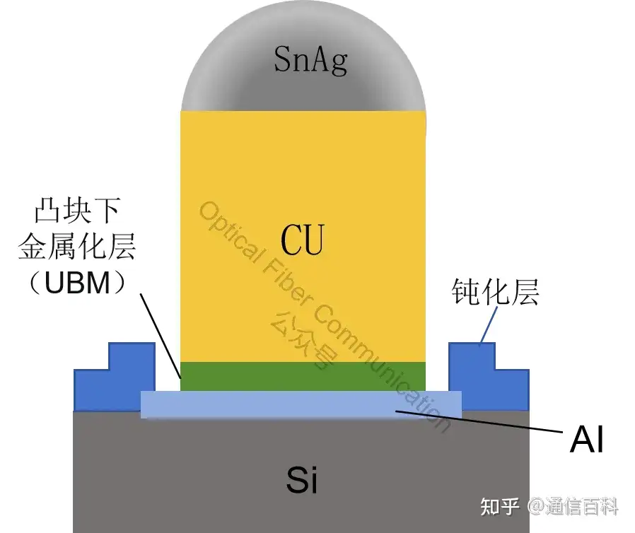
The diameter of a Cu Pillar is usually between tens of um and about 100um. Since copper does not melt during reflow soldering, it does not collapse and can maintain a very stable interconnect height.
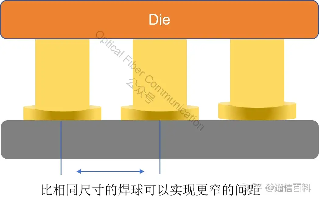
At present, it has been widely used in high-density flip-chip packaging.
But as advanced packaging continues to develop toward 3D stacking and heterogeneous integration, the requirements for interconnect density have reached unprecedented heights.
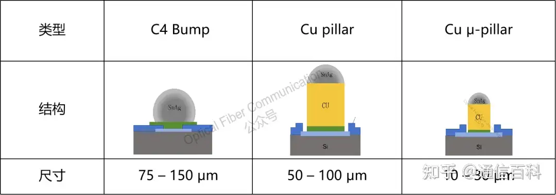
At this point, Cu Pillar technology must further evolve to μ-bumps, that is, Cu μ-Pillar (micro copper pillar), whose diameter further shrinks to 10 to 30um.
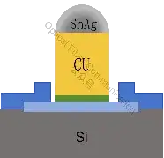
This structure can adapt to extremely high-density packaging requirements, such as 2.5D/3D IC integration and HBM stacking scenarios. There are related μ-bump applications in several CoWoS types.
For example, CoWoS-R packaging:
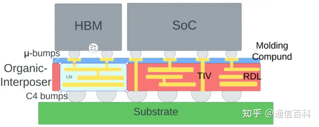
Generally speaking, in the highest-end 3D IC and 2.5D CoWoS packaging, when we mention “μ-bumps”, we often refer to the “Cu μ-Pillar” structure.
Let us summarize with a table:

Huawei HiSilicon’s Hi-ONE silicon photonics engine integrates more than 2000 devices on chip. Judging from the integration density and technology trend, we infer that it should use the more advanced Cu μ-Pillar technology.
Thanks for reading!
Related Reading
- How Did the Road from OTN to Flexible FlexO Packaging and Multiplexing Unfold?
- What Are the Packaging Processes for Optical Modules?
- Several Advanced Packaging Technologies
Enjoy this article?
Subscribe to get new optical communication insights delivered to your inbox. Free, unsubscribe anytime.