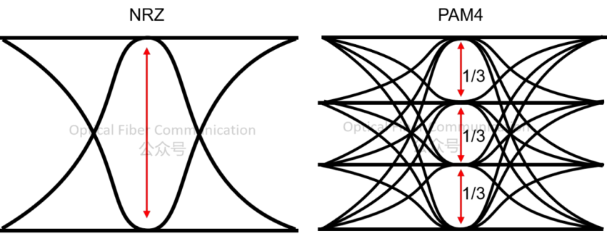
The eye diagram is used to judge whether a signal is good or bad. It can help us see the amplitude noise, timing jitter, and inter-symbol interference in the signal.
How is it generated?
The device first captures a segment of the actual signal, and then cuts the signal into many small segments according to the bit period recovered from the clock. Next, these small segment waveforms are aligned in time and stacked layer by layer for display.

That is, using the persistence method, the previous waveform traces are retained and new ones are continuously overlaid, eventually forming a superimposed statistical graph.
Breaking it down, three symbols have eight combinations: 000, 001, 010, 101, 011, 111, 110, 100. Taking the 0001011100 bit stream as an example.
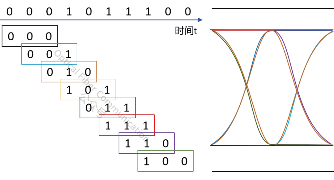
The eye diagram we actually see in optical module testing is the result of aligning and superimposing the waveforms of thousands upon thousands of bits within the time width of one bit.
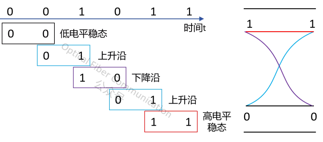
What happens if only two symbols are superimposed?
If there are two symbols, 0 and 1, there are four combinations: 00, 01, 10, 11. For example, receiving the 001011 bit stream would produce an “X”-shaped graph.
On the vertical voltage axis, noise is reflected in the form of voltage noise, and on the horizontal time axis, it is reflected in the time domain (jitter).
Under the same conditions, the eye height of each eye of PAM4 is only about 1/3 of that of NRZ, which means its signal-to-noise ratio is about 9.5 dB worse.
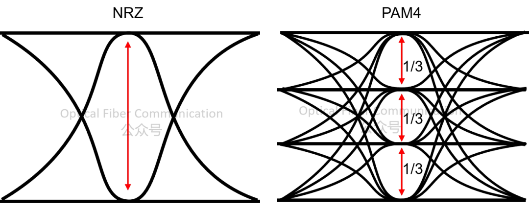
So how do we make the PAM4 eye diagram open wider?
There are only two directions: raise the eye height, or widen the eye width.
For lasers or modulators, within their linear operating range, increasing the drive current or voltage can increase the output amplitude, thereby increasing the eye height.
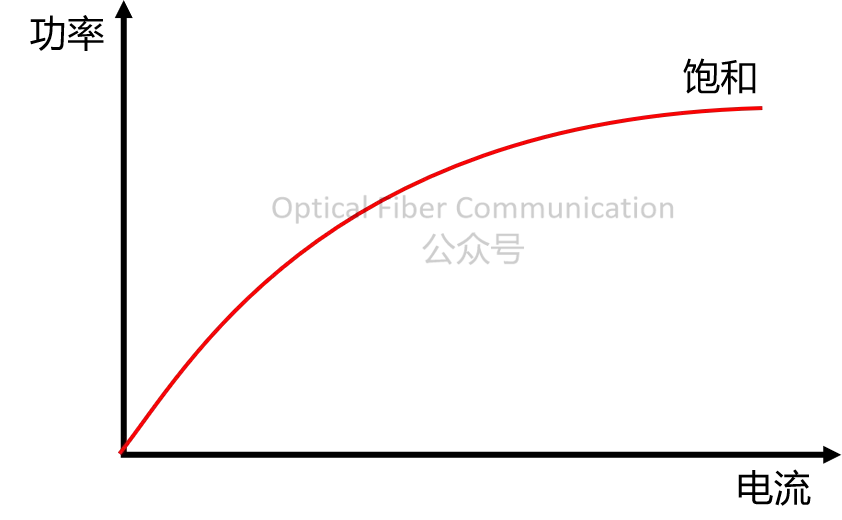
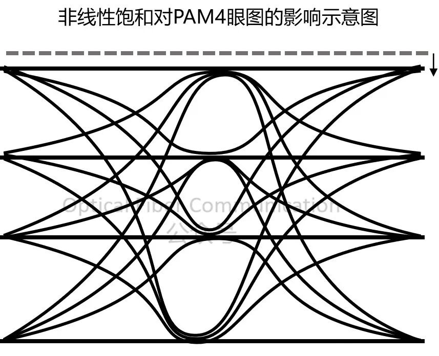
But there is a key point here: the current must not exceed the optimal operating point. Once exceeded, the device will saturate or distort, which instead leads to a decrease in eye height and distortion of the eye diagram.
Then the horizontal eye width can be increased, which can be achieved through the rise time or fall time of the signal.
In other words, the larger the bandwidth, the more high-frequency components the system can pass, the faster the signal transitions, the narrower the pulse, and the larger the eye width.
For DFB lasers and the like, their bias current directly affects the system bandwidth.
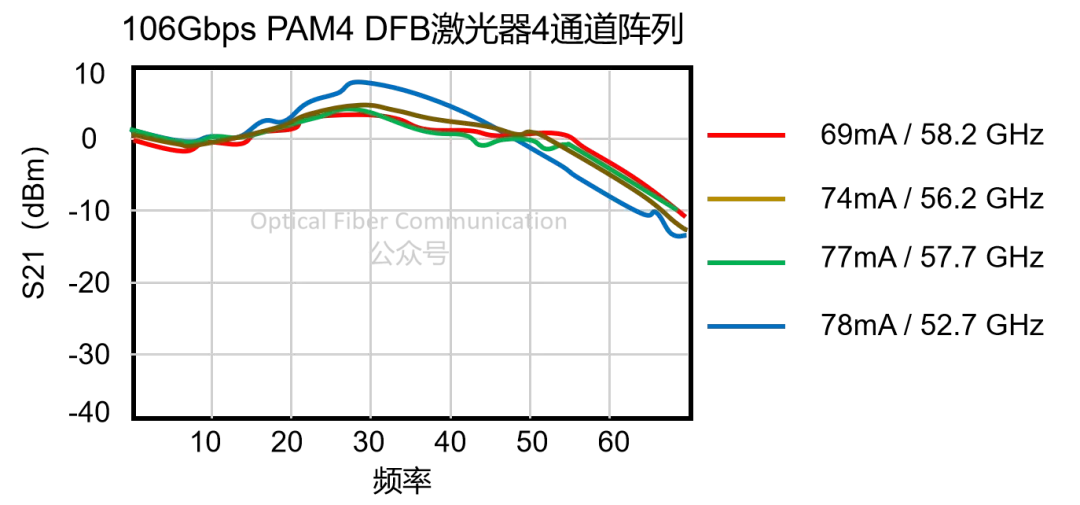
For small-amplitude transitions in PAM4 signals, such as jumping from -1 to +1, the signal energy itself is small and the change is slow, and they are particularly sensitive to the small-signal bandwidth of the system.
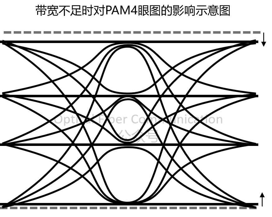
If the system bandwidth is insufficient or the high-frequency response is attenuated, the rise/fall time of the small signal will be noticeably slower. The result is pulse broadening and severe inter-symbol interference.
Thank you for reading. If there is any inaccuracy, please feel free to point it out.
Recommended Reading:
- Huawei: 100G Bandwidth GeSi Photodetector for C+L Band with Stress Layer
- Optical Modulation Amplitude (OMA)
You can add WeChat WaytoICT to be invited to join the Semiconductor & Optical Device Industry Chain Group 2.
Welcome to join our community to obtain a large number of high-value technical documents and trend research reports in the fields of semiconductor chips / optical devices / optical modules!
Welcome to follow us!
Enjoy this article?
Subscribe to get new optical communication insights delivered to your inbox. Free, unsubscribe anytime.