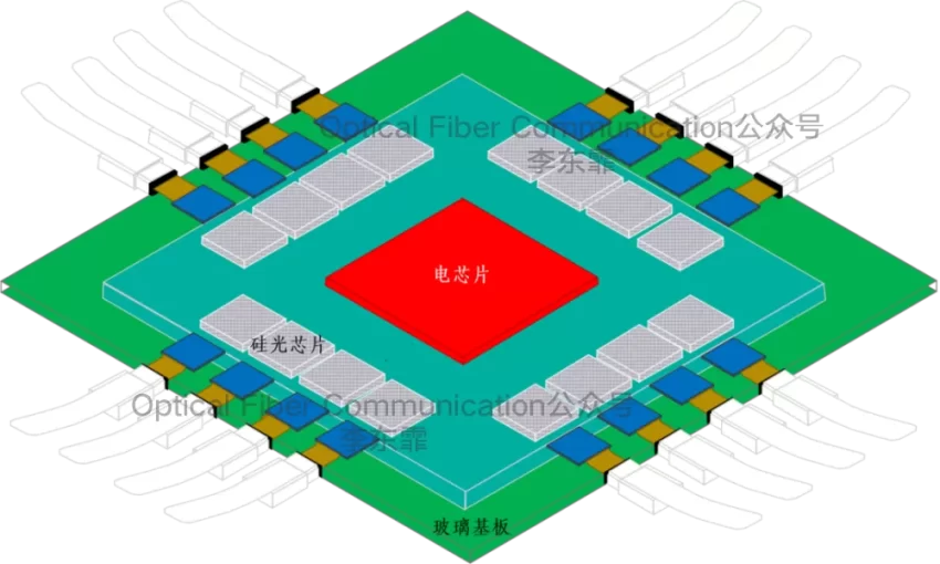
Glass substrates have been talked about for several years, and it can be said that they only truly began to land in 2026.
Previously in our article “Corning: Progress on Flip-Chip CPO Packaging Process for Silicon Photonics PIC Glass Substrates“, some friends left messages asking when mass production would be possible. I think one of the key prerequisites depends on when the glass substrate can land.
Intel’s Clearwater Forest has entered mass production and shipment, becoming the world’s first high-volume processor to use glass substrates. TSMC’s CoPoS glass substrate pilot line is expected to be completed in the middle of this year. Samsung and Absolics’ fabs are also breaking ground in parallel.
Mainstream manufacturers are all betting on glass substrates, and the most important reason is that organic substrates have truly reached their physical limits.
But glass itself does not conduct electricity, and the vertical high-speed signals between the upper and lower layers of the chip, chiplets, and HBM can only be conducted through TGV (through-glass via) glass vias. At present, this process cannot yet produce stable qualified products; it depends on which company can first raise TGV yield to the standard for mass production.
Over the past decade, advanced packaging has relied on organic substrates, that is, ABF build-up substrates. They are cheap, mature, and have a complete supply chain.
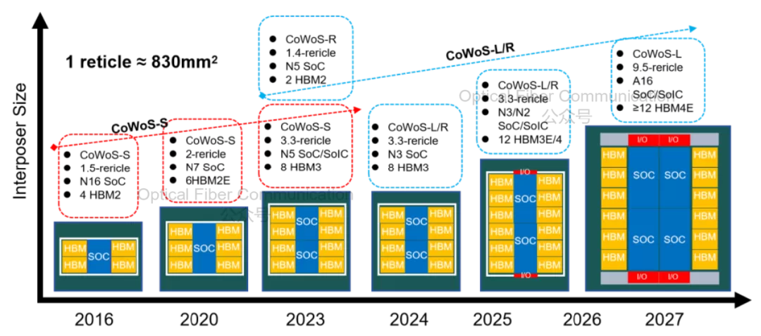
But AI has pushed package size to several times the reticle. CoWoS (Chip-on-Wafer-on-Substrate) has already exceeded 5 times the reticle area, and the next generation will go to more than 9.5 times.
TSMC: CPO Packaging Process Based on Silicon Photonics TDV Process
Therefore, ABF faces three major problems: warpage, inability to increase wiring density, and large high-frequency loss. Moreover, the thermal expansion coefficient of resin differs too much from that of silicon. When the area is large and the temperature is high, it warps, and the subsequent RDL redistribution wiring simply cannot proceed.
In comparison, the CTE of glass can be tuned close to that of silicon, with a flat surface and low dielectric loss.
The effective area of a 12-inch silicon wafer is about 72900 mm2; a 515×510 mm glass panel has an area of 262700 mm2, 3.6 times that of a wafer; a 650×550 mm panel has an area of 357500 mm2, 4.9 times that of a wafer.
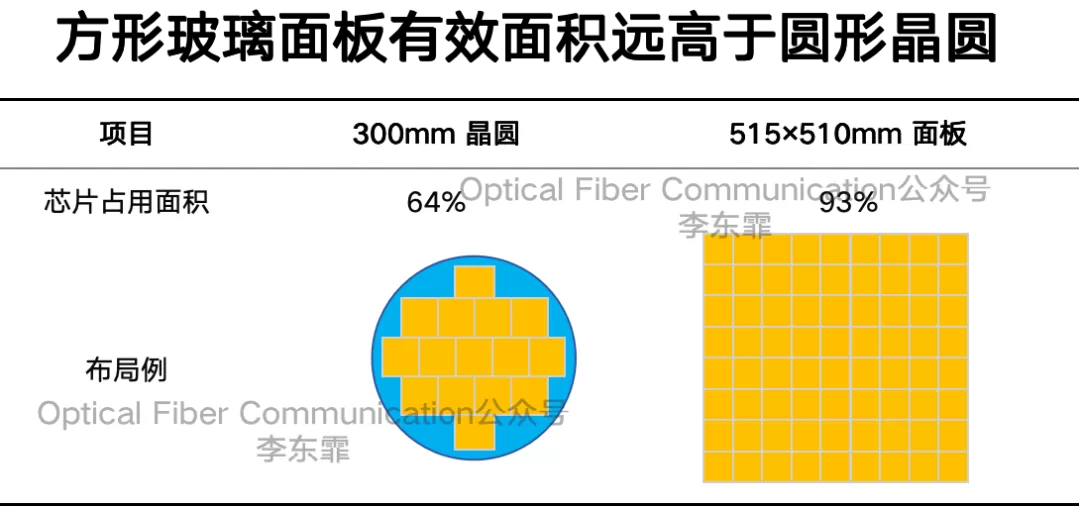
Under the same process, the number of effective packages produced by a square panel is far higher than that of a round wafer, so the unit cost is significantly amortized.
As mentioned earlier, glass itself is an insulator. Without drilling holes and filling metal, it is just a piece of glass. For signals to pass vertically, TGV must be used to drill high-aspect-ratio vias and then fill them with copper. So its yield, cost, and density are all stuck at this step.
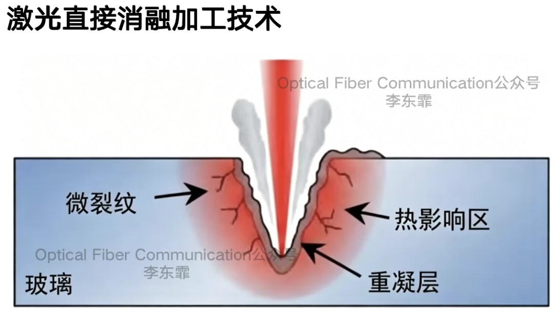
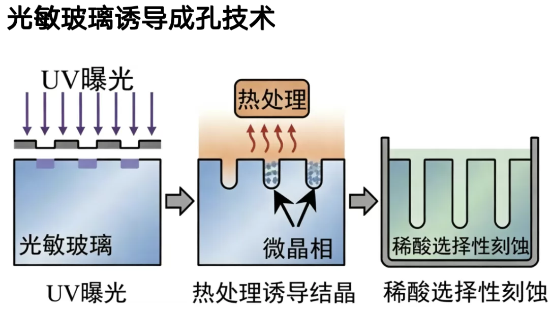
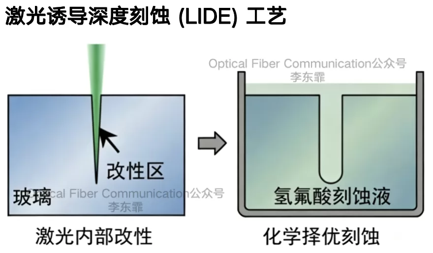
At present, there are mainly four drilling processes: mechanical drilling, laser ablation, photosensitive glass vias, and LIDE.
Among them, mechanical drilling has a minimum hole diameter greater than 150 um and an aspect ratio less than 5:1, with severe edge chipping, and is basically out of the running.
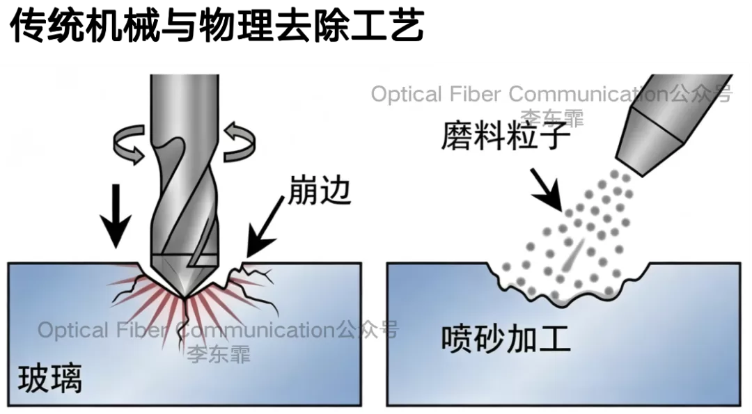
Laser ablation has a hole diameter of about 30 um and an aspect ratio of about 10:1, but leaves microcracks and a recast layer.
Photosensitive glass has a hole diameter of about 25 um and an aspect ratio of about 20:1, but the material is limited.
LIDE (Laser-Induced Deep Etching) can achieve a hole diameter of less than 10 um and an aspect ratio greater than 50:1, with high batch efficiency. Its two-step process avoids mechanical and thermal stress, and it is recognized as the route with the greatest mass-production potential, which Intel is promoting.
After drilling, there is also metallization filling and RDL. Whether copper can be filled in without voids and whether fine-line wiring can be produced on the surface directly determine the quality of the electrical connection. Corning, Atotech, and DuPont are all competing here.
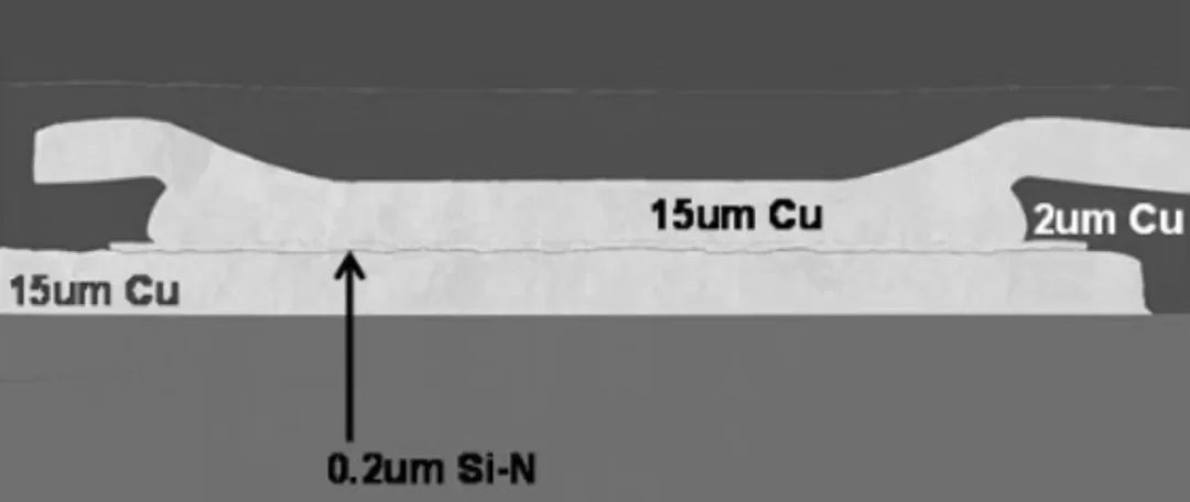
Glass substrates are divided into two routes.
The first route is the TGV interposer, used to replace the silicon interposer. Using a glass interposer to carry multiple chips, it benchmarks against the silicon interposer in CoWoS.
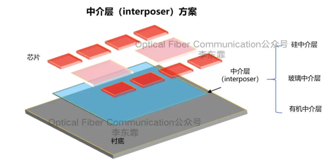
Interposer, Silicon Bridge, and PIC/EIC Stacking Solutions
TSMC’s CoPoS follows this panel-level route. The pilot line equipment will be completed in the middle of this year, with mass production planned for the second half of 2028. The first product is targeted at NVIDIA’s Feynman. Samsung is testing the use of glass in HBM4 stacked packaging.
The second route is the glass core, used to replace the organic packaging substrate. In early 2026, Intel shipped the world’s first high-volume processor using a glass core, namely Xeon 6+ Clearwater Forest.
It adopts a 10-2-10 structure, with a central glass core of about 800 microns, and 10 layers of high-density RDL stacked on the top and bottom. The CTE of the glass core is almost identical to that of silicon, so when the core runs at full speed and generates heat, it does not warp due to thermal stress.
These two routes are not mutually exclusive, but rather two entry points through which glass comprehensively penetrates advanced packaging, from interposer to carrier board.
For those concerned with high-speed data transmission, the application of glass substrates worth noting is not in the CPU, but in CPO.
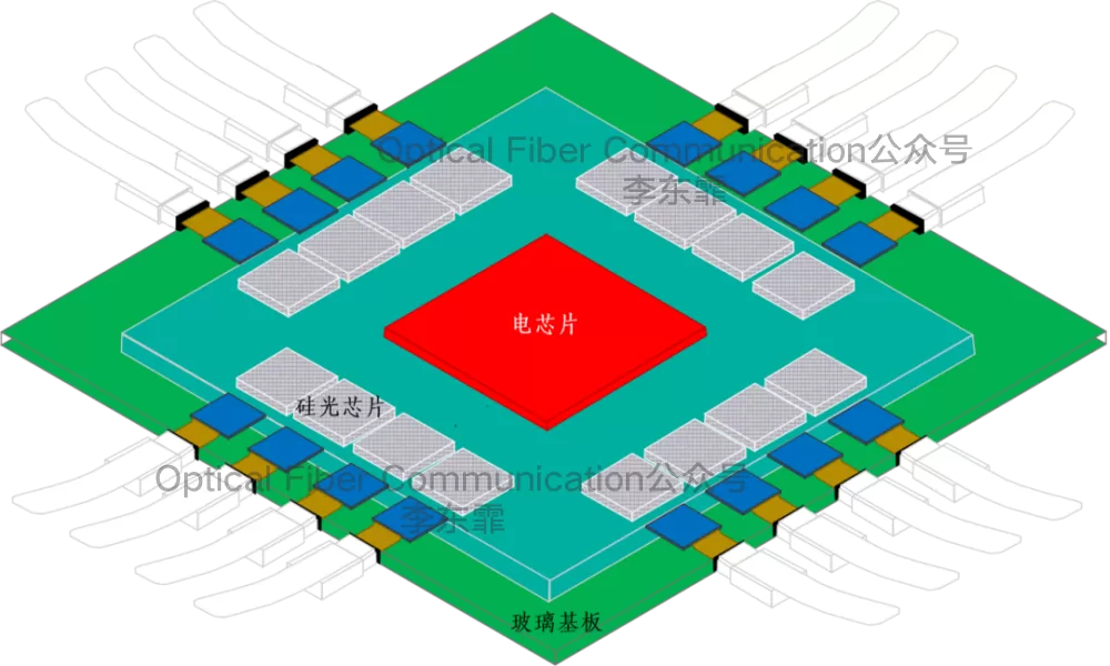
Corning: Low Bending Loss Process and Improvement of Glass Waveguides for CPO
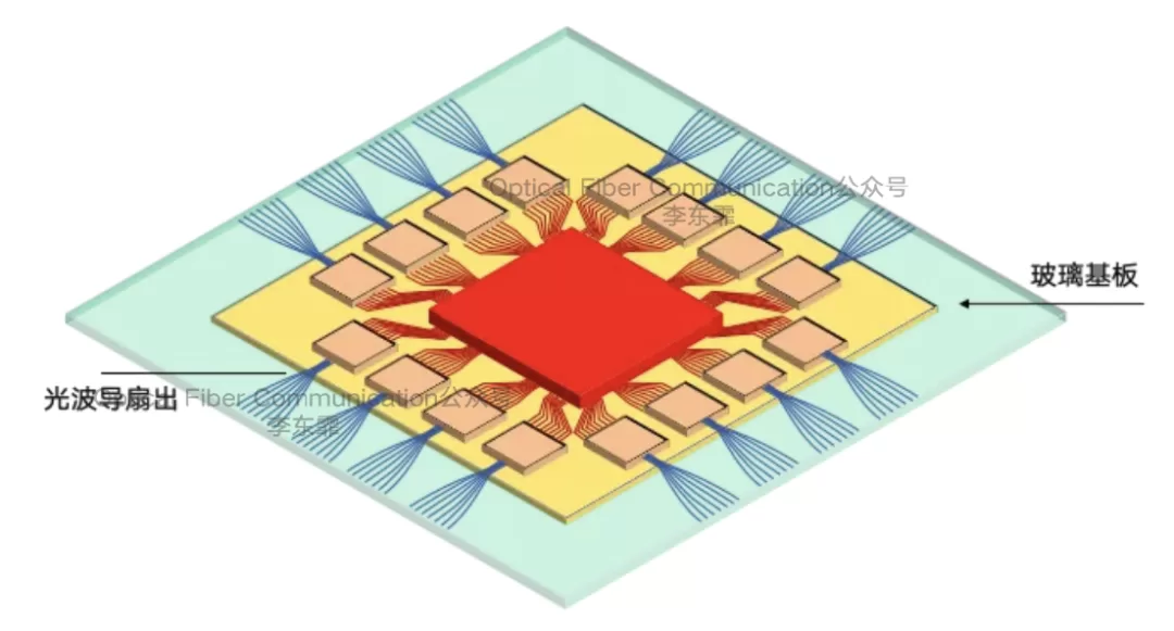
CPO Packaging Structure Based on Glass Carrier Board
The Singapore Institute of Microelectronics (IME / A*STAR) proposed a direct double-sided RF probe measurement method at ECTC 2026, raising the test frequency band of the four types of vertical interconnect structures – SUB-VIA, TMV, TSV, and TGV – to above 110 GHz, comparing the 448 Gbps single-channel transmission performance of each structure.
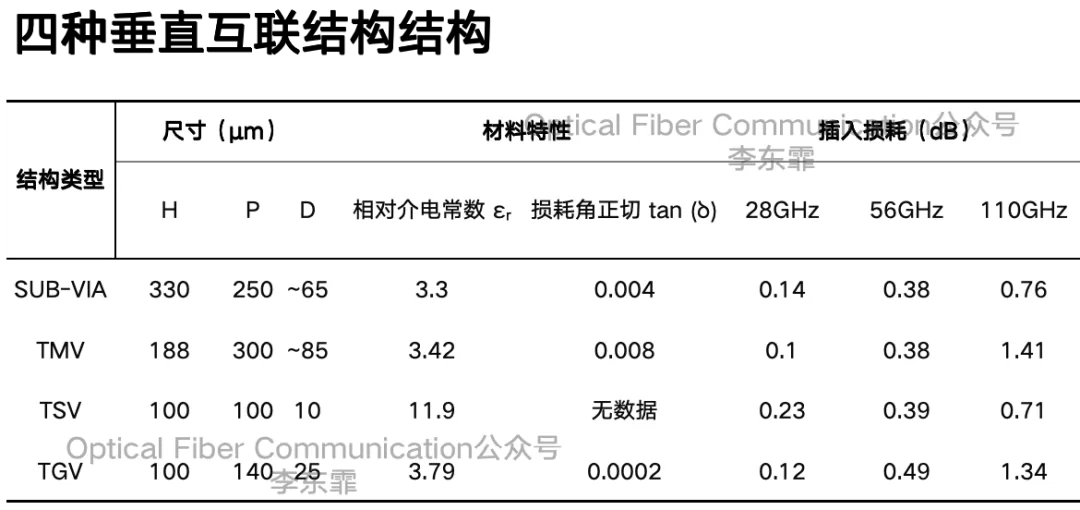
The dielectric loss tangent of TGV is 0.0002, the lowest among the four structures. The dielectric constant of the silicon substrate of TSV is as high as 11.9, and signal leakage begins at low frequencies.
At 112 GHz, the differential insertion loss of TGV is 0.13 dB, that of TSV is 0.37 dB, SUB-VIA is 0.60 dB, and TMV is 0.87 dB.
In addition, the pitch of TGV can directly match the EIC pad specification of 125 um, without the need for additional fan-out wiring.
However, the overall mass-production yield ramp of TGV is currently slow, and there is still a distance from stable large-scale mass production.
Glass is hard and brittle, and the back-end RDL process can easily cause cracking at the board edge. The industry has used finite element analysis to calculate this problem. Fused silica, borosilicate glass 33, D263, Gorilla Glass, and ceramic glass differ greatly in crack resistance, and board thickness, edge margin, ABF material, and copper content all affect crack propagation.
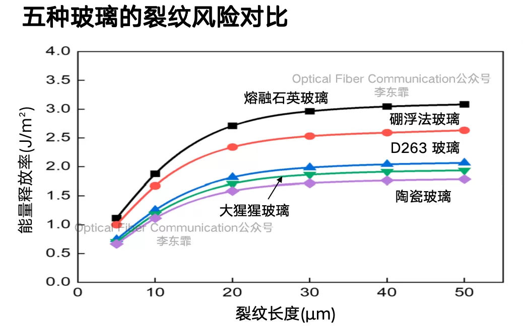
The interface delamination of the three-layer structure of substrate, adhesive layer, and chip also needs to be controlled by repeated calibration of the cohesive zone model. That is to say, switching to a glass substrate is not just a matter of replacing one material, but the entire process needs to be re-established.
Then there is the warpage problem, which is actually an advantage of glass.
The flatness of glass substrates produced by Corning’s fusion-draw process is an order of magnitude higher than that of organic substrates. In a 508×508 mm panel, the warpage of glass is only one-third that of organic substrates, and Corning has long reserved patents related to layered structures and anti-warpage technology.
If there is any inaccuracy, please feel free to point it out.
Welcome to join our community to obtain high-value technical documents, trend research reports, and various supply-demand business opportunities in the fields of semiconductor chips / optical devices / optical modules.

If you are interested in semiconductors / optical devices / optical modules / optical fiber communication, etc.
Welcome to follow us!
Related Reading
- Glass Substrate: Pluggable Connection Solution in CPO Packaging
- Mitsubishi: From High-Mesa Structure to Hybrid Glass Substrate and FC+WB High-Speed EML
- How Did the Packaging and Multiplexing Path from OTN to Flexible FlexO Go?
Enjoy this article?
Subscribe to get new optical communication insights delivered to your inbox. Free, unsubscribe anytime.