Related Reading: NVIDIA: Interconnect Architecture and Technical Analysis of Integrated Silicon Photonics CPO | Alibaba Cloud: NPO Evolution Route and Deployment Strategy for AI Cluster Optical Interconnect | Baidu: Evolution and Response Strategy of AI Cluster Optical Interconnect
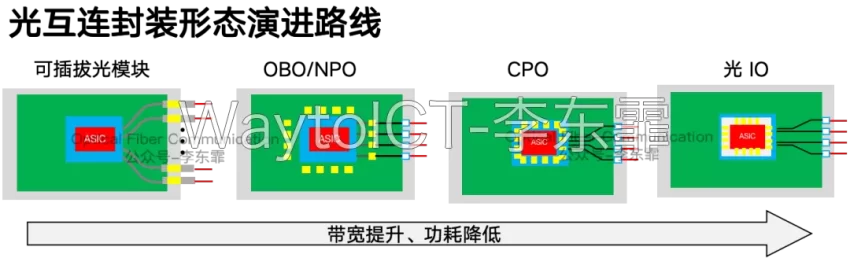
The industry usually divides optical interconnect into two levels – device-level and chip-level – based on the integration of the optical engine with the computing chip, as well as the electrical signal transmission distance.
In device-level interconnect, electrical signals travel meter-level or even decimeter-level distances; in chip-level optical interconnect, this distance is compressed to the cm and mm level, forming a three-stage evolution route.
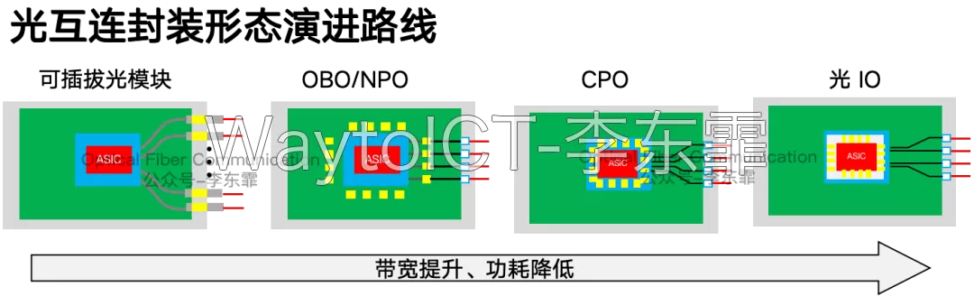
Among them, CPO integrates the optical engine with the xPU on the same substrate or interposer, shortening the electrical signal transmission path to the greatest extent and completing the optoelectronic conversion directly on the chip side.
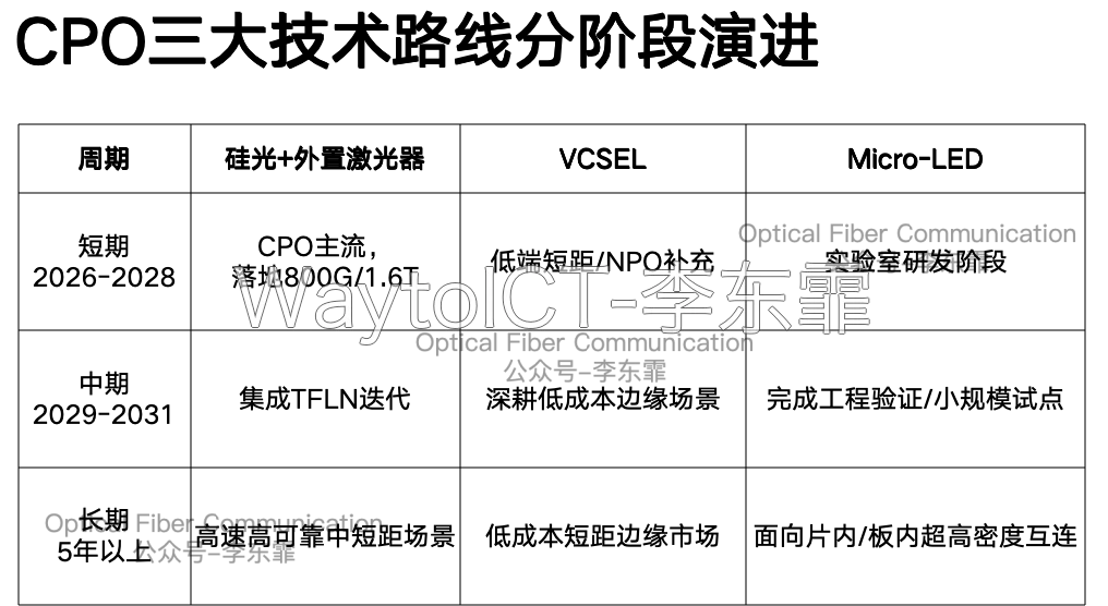
At present, the global CPO industry is mainly divided into three technical routes: external light source ELSFP plus silicon photonics optical engine, VCSEL array optical engine, and Micro-LED array optical engine.
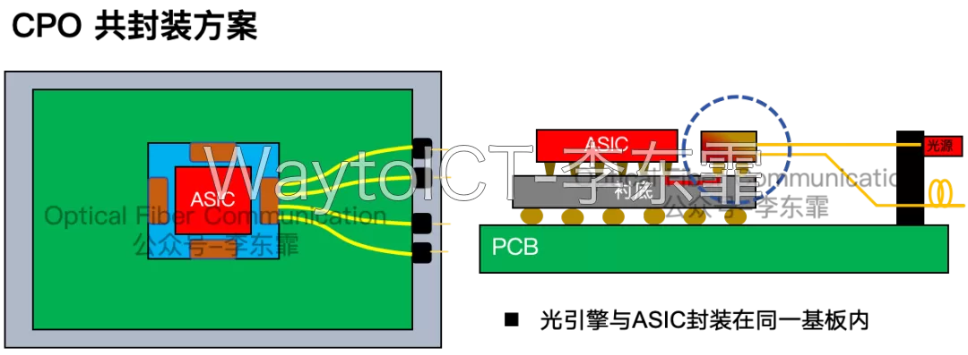
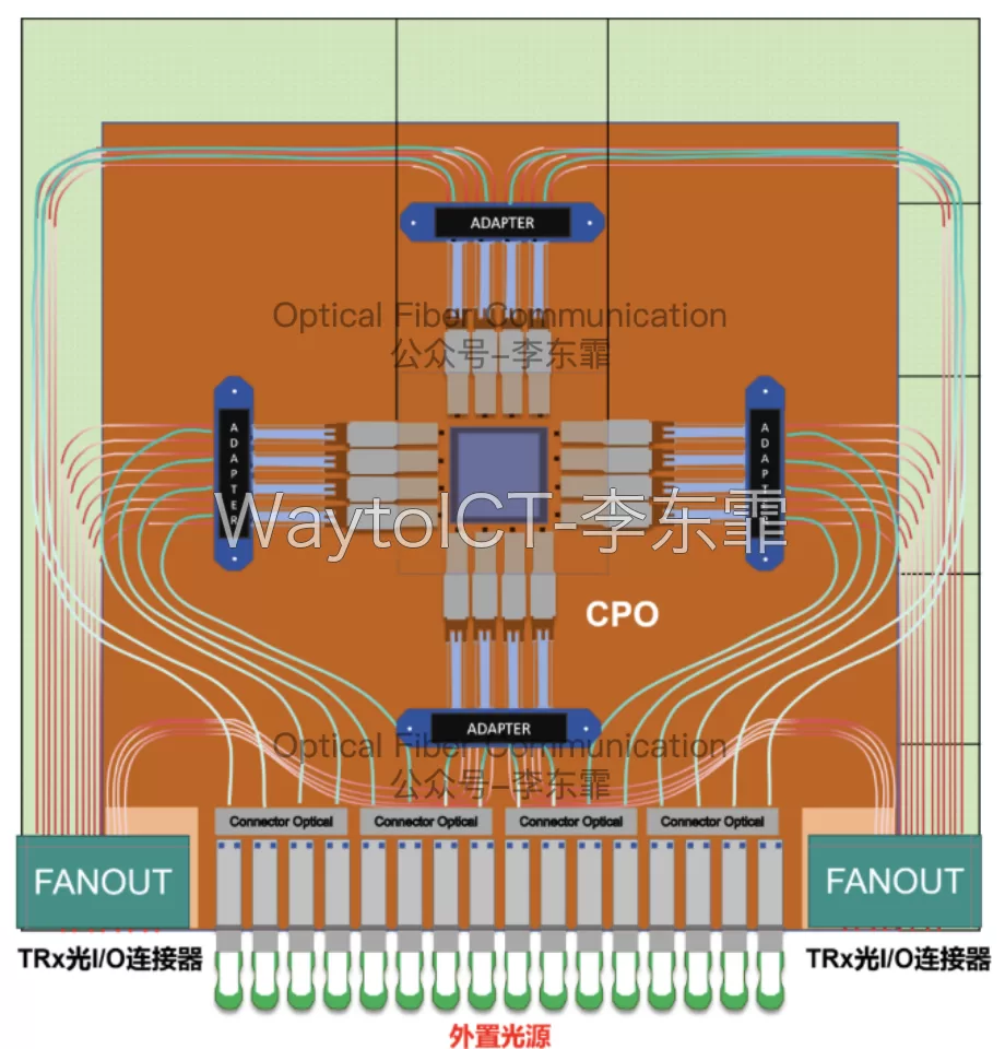
Route 1: External Light Source ELSFP + Silicon Photonics Optical Engine
The current mainstream industry route is the external laser source plus silicon photonics optical engine. The optical engine obtains continuous-wave laser light through the ELSFP external laser source module, and hands it to a dedicated modulator to complete the electro-optic signal conversion, which is an indirect modulation scheme.
Related solutions: Ericsson: Semi-Deterministic Compensation Scheme for CPO External Light Source without Polarization-Maintaining Fiber, Furukawa: Progress on ELSFP External Light Source Supporting CPO, NVIDIA: CPO External Light Source Coupling Scheme with Polarization Tracker, ZTE: Reliable Installation and Heat Dissipation Scheme for CPO External Light Source.
The modulators used for the external light source ELSFP mainly include two types of schemes: MZM and MRM.
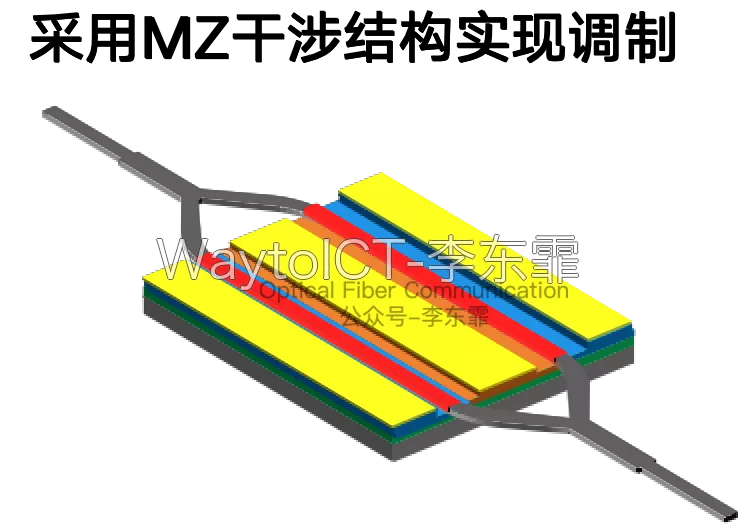
Among them, the MZM (Mach-Zehnder modulator) consists of an input Y-branch splitter, two parallel waveguide arms, and an output Y-branch combiner. By applying voltage through electrodes to change the waveguide refractive index, a phase difference is produced between the two arms, and then optical intensity modulation is achieved through interference.
Related solutions: Polaris: 400G Silicon Photonics MZM Modulator Based on Ferroelectric Nematic Glass, Coherent: Single-Channel 400G PAM4 Pure-Silicon MZM Modulation Scheme, GlobalFoundries: Silicon Photonics MZM Modulator Scheme for Single-Wavelength 200G.
The advantage of MZM is its wide operating wavelength range, strong thermal stability, long transmission distance, and support for multi-wavelength WDM.
However, its device size is relatively large, usually at the mm level, and the drive voltage is also large, so the number of channels that can be integrated on a single chip and the room for energy-efficiency improvement are limited.
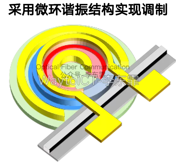
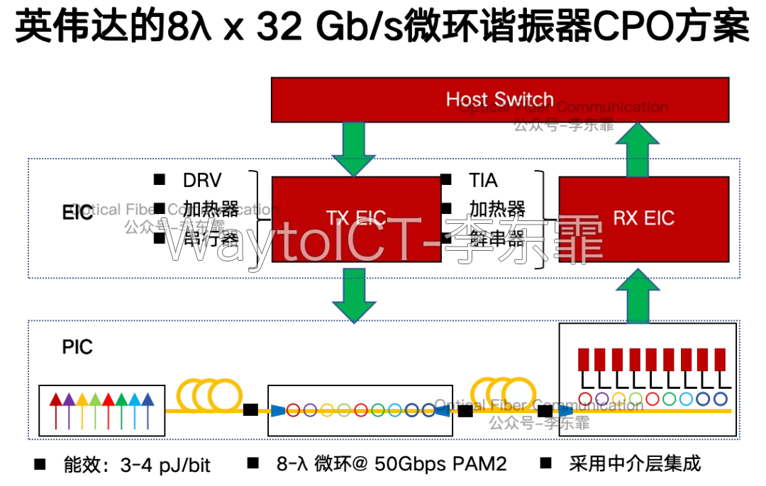
The MRM (microring modulator) adopts a ring resonator structure, formed by the coupling of a ring waveguide and a bus waveguide. By applying voltage on the PN junction of the microring to change the effective refractive index, the resonant wavelength shifts, achieving optical intensity modulation.
The device size of microring CPO can be made extremely small, with low drive voltage. Through the combination of multi-microring arrays and WDM, a single PIC can support over a hundred high-speed optical channels, making it the current mainstream modulator scheme for CPO technology.
Related solutions: NVIDIA: Low-Sensitivity Microring Resonator for Reducing Process Errors, Lightmatter: 16-Wavelength 800G BiDi Microring Silicon Photonics CPO Solution, HiSilicon / Intel: SiN-SOI Microring Modulator for CPO, Microring Resonator: Coupling, Modulation and WDM.
The shortcoming of the microring scheme is that the resonant wavelength is highly sensitive to temperature, and wavelength drift is prone to occur at high temperatures, so temperature control and thermal compensation design must be matched.
Route 2: VCSEL Array Optical Engine
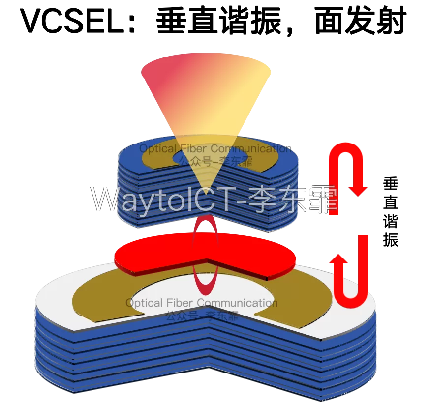
The second route is an optical engine based on a VCSEL array. VCSEL, the vertical-cavity surface-emitting laser, does not need an independent modulator and is a direct modulation scheme, directly completing electro-optic signal conversion by changing the injection current.
Because light is emitted vertically upward directly from the chip surface, the spot is circularly symmetric and insensitive to reflected light. Usually only one lens is needed to efficiently send light into the fiber, and the isolator can be omitted, so the structure of VCSEL CPO is simplified.
At the same time, VCSEL is naturally suitable for making arrays, which facilitates large-scale integration, such as Bosheng’s 3×12 VCSEL array.
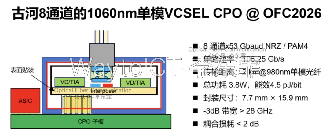
In addition, Furukawa Electric’s 8-channel VCSEL/PD array based on organic substrate integration arranges the transimpedance amplifier and VD chip symmetrically, uses a 24-channel MT connector for the optical port, and integrates a plastic microlens array to achieve efficient coupling.
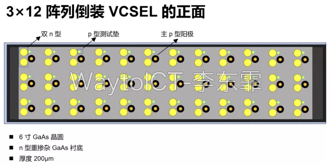
Related solutions: Coherent: Wide and Slow VCSEL CPO Solution and Energy Efficiency Evaluation, Furukawa Electric: Progress on Single-Mode VCSEL Array CPO Technology, Sony: Full-Temperature-Range 200G Multi-Mode VCSEL Solution, Bosheng: Back-Emitting Multi-Mode VCSEL 1.6T Array Solution for CPO/NPO, Lumentum: VCSEL Polarization Locking Scheme.
The VCSEL-based CPO solution has a simple device structure and mature process, with lower mass-production cost. The direct modulation architecture brings small loss, and the per-bit power consumption performance is also excellent.
However, there is lattice mismatch between gallium arsenide and silicon-based CMOS chips, making deep co-packaging difficult and the hybrid integration yield not high.
In addition, it is difficult to improve the single-channel rate, and high-temperature stability is poor, so it cannot support ultra-high-speed transmission of over 200 Gbps per channel.
The loss of optical signals during transmission is also relatively high, with an effective transmission distance of only tens of meters, unable to meet the long-distance networking needs across cabinets.
Route 3: Micro-LED Array Optical Engine
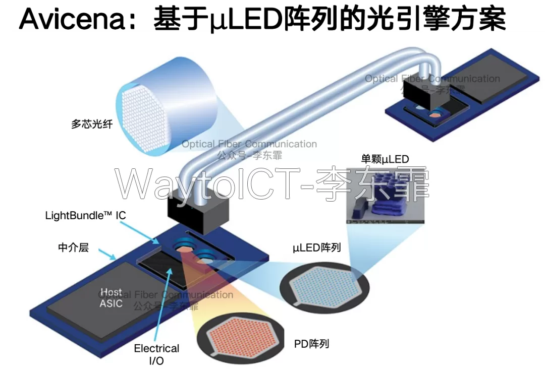
The third route is an optical engine based on a Micro-LED array. Micro-LED, sometimes written as uLED, is a micro light-emitting diode fabricated with gallium nitride as the substrate to produce micron-scale light-emitting units, which can form a two-dimensional high-density array.
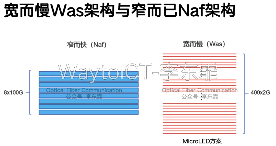
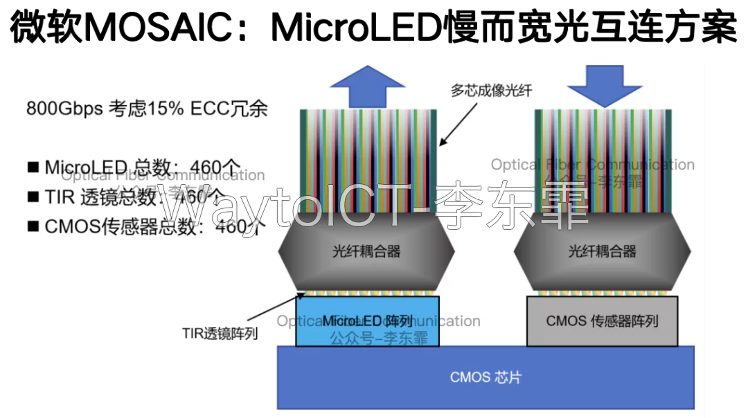
Micro-LED is a “wide and slow” technical idea of parallel superposition of multiple low-rate channels, relying on a large number of low-rate channels to achieve ultra-high total bandwidth, naturally supporting space-division multiplexing.
For example, Microsoft’s MOSAIC scheme based on the Was slow-and-wide architecture can deploy 460 Micro-LEDs (including redundancy) on one 800Gbps link, arranged in a 20×20 grid, with each LED at a rate of 2Gbps (Micro-LED and Was Architecture: Microsoft and Avicena Micro-LED Solutions).
Among the three routes, the Micro-LED CPO solution has the highest ceiling: the strongest two-dimensional array integration capability, with bandwidth density that can exceed Tbps/mm2; the link power consumption potential can reach sub-pJ/bit, with energy efficiency superior to silicon photonics and VCSEL.
The main challenge of Micro-LED at present is unstable modulation response and large distortion at rates of 100 Gbps and above; the gallium nitride integration process is not mature, and the yield is low.
At the same time, attenuation failure is prone to occur under long-term high-load operation, and reliability has not yet reached industry requirements.
Summary
In general, the three types of schemes will ultimately form a long-term differentiated coexistence.
The silicon photonics plus external laser solution will continue to serve as the core mainline of CPO, VCSEL will play its value in niche markets, and Micro-LED is worth long-term tracking.
Thank you for reading! If there is any inaccuracy, please feel free to point it out.
The compilation of reports on optical chips, optical devices, and optical modules (OFC2026), printed in color and bound in A4, comes in two volumes totaling about 525 pages and about 200,000 words. Please contact us to order if needed, at a reasonable price!
WeChat contact: WaytoICT
Extended Reading
- Pluggable, OBO, NPO and CPO
- CPO and 2.5D/3D Advanced Packaging
- Marvell: Packaging Technology Evolution Path for Ultra-CPO
Enjoy this article?
Subscribe to get new optical communication insights delivered to your inbox. Free, unsubscribe anytime.