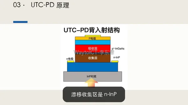
This 2-minute-40-second video explains the uni-traveling-carrier photodiode (UTC-PD): why the conventional PIN encounters a bandwidth bottleneck, how the UTC-PD bypasses it, and how the waveguide-type structure improves absorption efficiency.
The Conventional PIN Detector
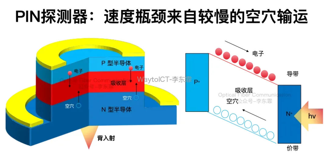
The conventional Si-PIN photodiode adds an I layer (intrinsic layer) between the P-type and N-type semiconductors, usually used as the absorption layer.
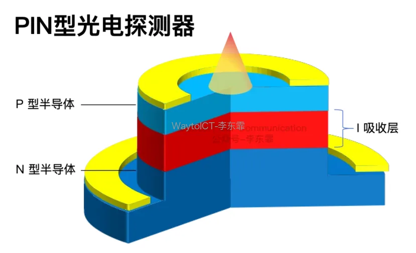
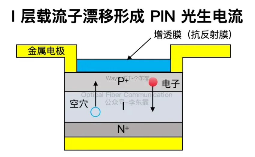
The I layer generates electron-hole pairs after absorbing photons. Under a reverse-bias electric field, electrons drift toward the N side and holes drift toward the P side, with both types of carriers together forming the photocurrent.
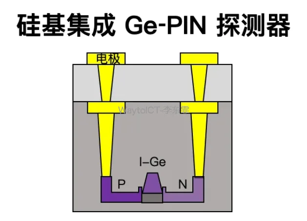
The absorption layer does not necessarily use silicon: the indium gallium arsenide PIN in the indium phosphide system uses InGaAs as the absorption layer; the silicon-integrated Ge-PIN detector uses a Ge thin film as the absorption layer.
The Bandwidth Bottleneck: Slow Holes
In a conventional PIN, both electrons and holes contribute to the photocurrent, and the speed at which they move toward the two sides in the depletion layer determines the photoresponse speed, that is, the bandwidth. Since the electron drift velocity is much faster than that of holes, the limitation on the carrier transit time mainly comes from holes.
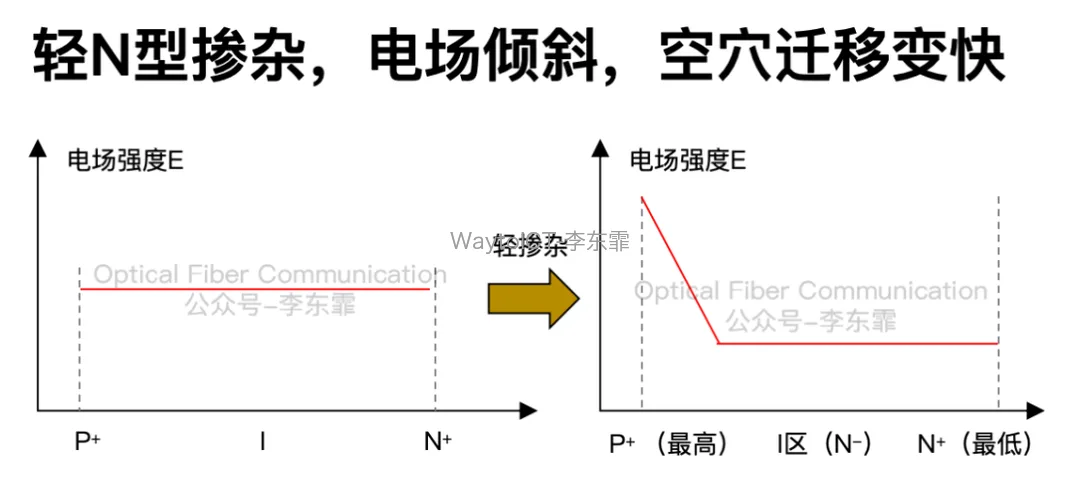
One way to make holes drift faster is to use light N-type background doping: the electric field in the depletion region is no longer flat and uniform, but gradually strengthens from the N side toward the P side, so when holes drift toward P+, they pass through a stronger electric field and drift faster.
UTC-PD: Letting Only Electrons Participate in the Photocurrent
Holes are always the main limitation on bandwidth and cannot be completely eliminated. A more thorough approach is to collect only electrons, letting electrons serve as the main carriers while holes do not participate in conduction.
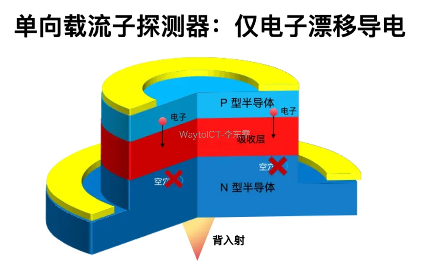
Under an applied voltage, the electron collection layer generates a strong electric field, and the photogenerated electrons move from the absorption layer to the collection layer, with the photocurrent basically generated entirely by electrons. The drift blocking layer blocks holes from entering the drift region, while electrons enter the drift layer and are ultimately collected by the collection layer.
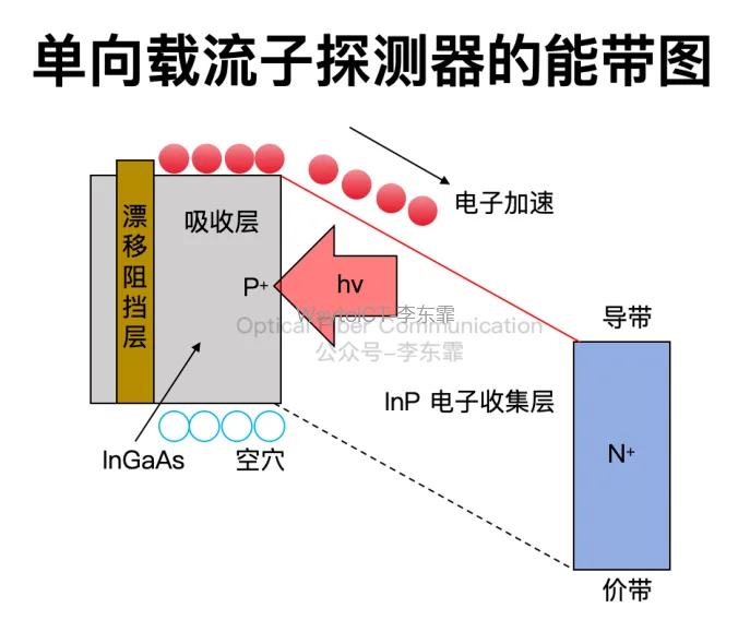
This detector, in which only electrons participate in the photocurrent, is the uni-traveling-carrier photodiode (UTC-PD for short). Unlike the conventional PIN, the UTC-PD separates the absorption region from the drift collection region: the absorption region is p+-InGaAs, and the drift collection region is n-InP.
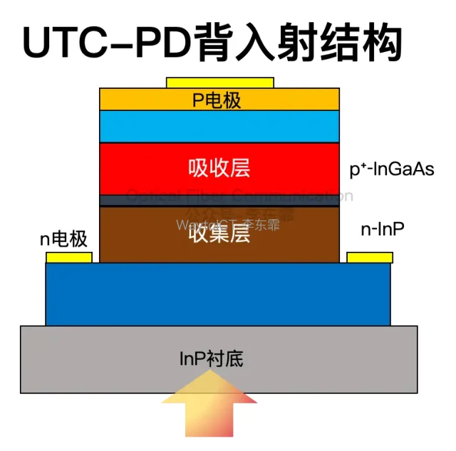
Holes do not need to pass through a long drift path, so the limitation of slow holes on bandwidth is eliminated, allowing a very high bandwidth to be achieved.
Waveguide-Type UTC-PD
Although shortening the carrier transit path can improve bandwidth, it also reduces optical absorption. The solution is to let light enter the detector by edge coupling, that is, the waveguide-type UTC-PD: the light is refracted when it enters the inclined surface, obliquely entering the absorption layer at a certain angle, which increases the light absorption area compared with direct back incidence.
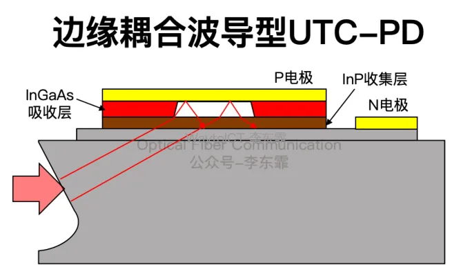
The video is produced by this site, narrated by Li Dongfei. To see the details of a particular section, just drag the progress bar.
Related Reading
- Huawei: C+L Band 100G Bandwidth Germanium-Silicon Photodetector with a Strain Layer
- Basics: Waveguide-Type Photodetector
- Basics: Uni-Traveling-Carrier Photodiode
Enjoy this article?
Subscribe to get new optical communication insights delivered to your inbox. Free, unsubscribe anytime.