Silicon can form waveguides and optical switches: using the plasma dispersion effect, applying an external voltage changes the carrier concentration and hence the refractive index, enabling silicon-based MZMs or microring modulators.
But silicon has no linear electro-optic effect, and modulation relies on carrier transport, making it hard to achieve high speed, low voltage, and low loss simultaneously.
So on the SOI silicon photonics platform, heterogeneous integration is often used to extend functionality. For example, heterogeneous integration of silicon and germanium can be used to make photodetectors.
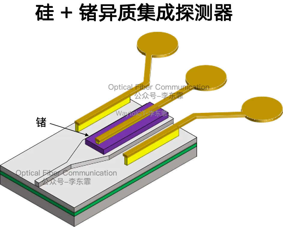
In addition, silicon is an indirect-bandgap semiconductor with very low emission efficiency, producing almost no useful light. So the silicon photonics platform also needs heterogeneous integration with III-V materials to make lasers, such as silicon-based InP lasers.
The situation is similar for thin-film lithium niobate (TFLN). TFLN can make passive devices such as waveguides, splitters, and microring resonators, as well as active devices such as electro-optic modulators and frequency combs, but TFLN likewise cannot make lasers — because lithium niobate is a wide-bandgap insulator, and its valence-band electrons are tightly bound to the atoms, so there are almost no free carriers to participate in radiative recombination.
Therefore TFLN also needs integration with III-V gain materials, and there are currently two main routes. The first is hybrid integration: the III-V gain wafer and the TFLN wafer are patterned independently, i.e., their waveguides, electrodes, and gratings are fabricated separately.
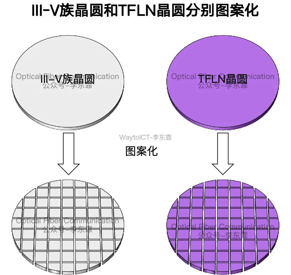
Because patterning is completed in the front-end, both sides can be tested and optimized independently before hybrid integration, which better ensures yield. After patterning, the III-V wafer is diced into individual chips, which are then attached to the TFLN chip through high-precision alignment and assembly.
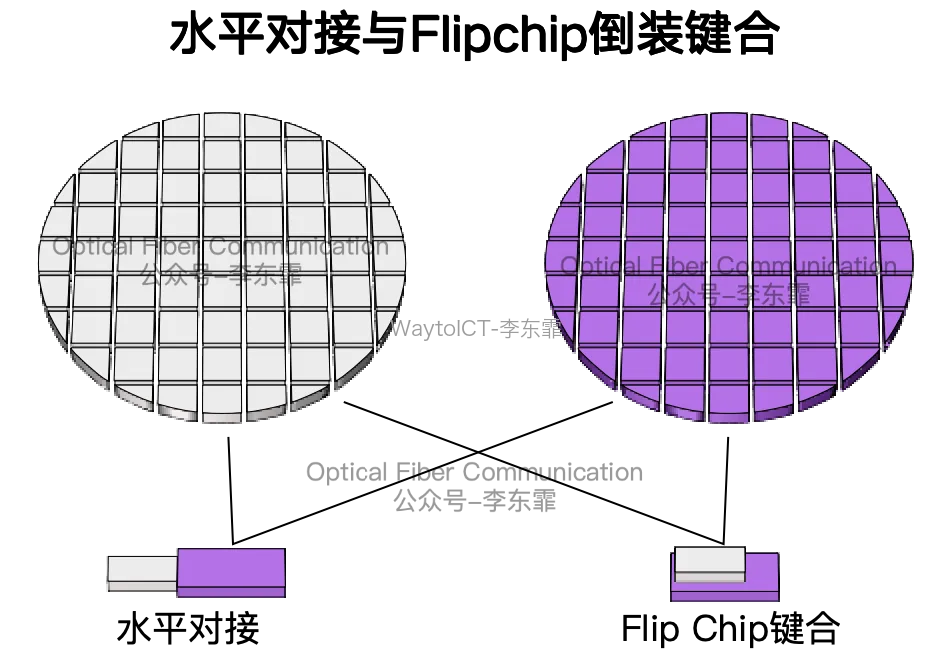
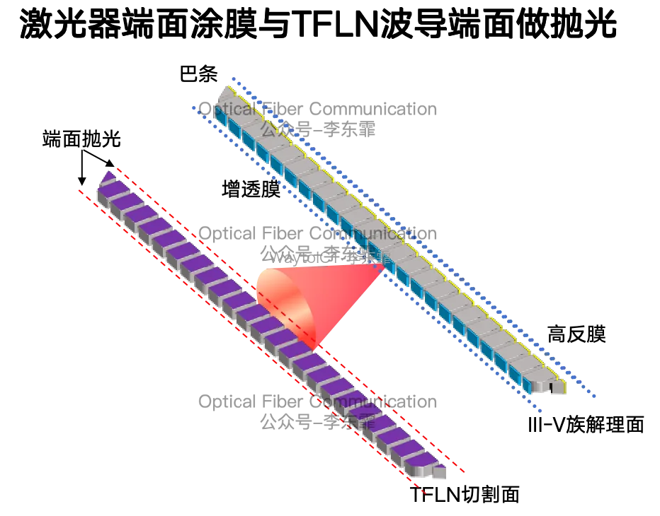
Hybrid integration is further divided by chip coupling method into horizontal end-face coupling and flip-chip bonding. To reduce coupling loss, the TFLN chip end face is usually polished to reduce scattering loss, while the III-V laser output facet is coated with an anti-reflection coating, and a spot-size converter is sometimes used to match the mode field.
Flip-chip bonding means placing the III-V chip with its active layer facing down, with pre-fabricated gold-tin solder bumps on the chip surface aligned to metal electrode pads on the TFLN chip surface, then forming robust electrical connections through thermocompression or reflow soldering.
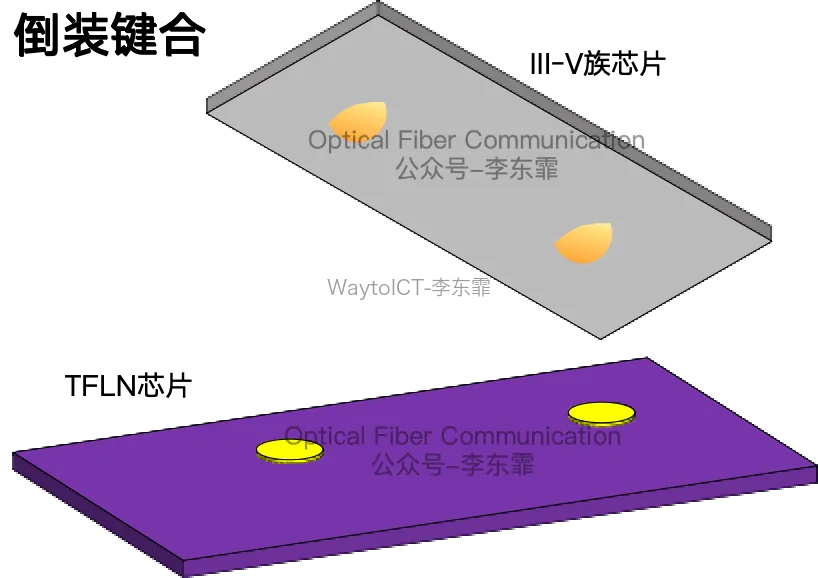
The advantage of flip-chip bonding is that no end-face coupling gap needs to be reserved on the TFLN chip side, so the entire wafer surface can be used for passive optical circuits such as splitting, modulation, and delay, achieving higher planar integration density.
Micro-transfer printing can also be used to hybrid-integrate III-V chips onto TFLN chips: a PDMS soft stamp picks up pre-fabricated laser thin films, moves them over the TFLN substrate, and after alignment attaches them to flat surface regions.
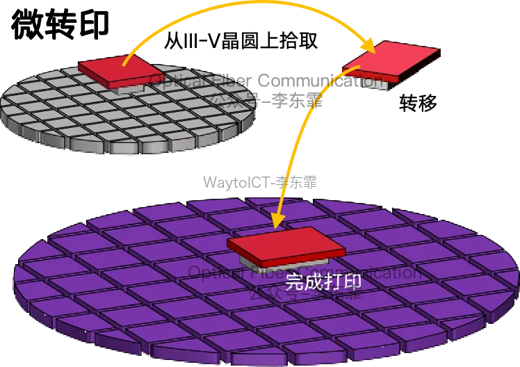
Micro-transfer printing can pick up and place multiple lasers simultaneously, which is favorable for mass production.
The hybrid integration described above all requires the TFLN modulator and the III-V laser to complete their waveguide, grating, and electrode fabrication independently at their respective foundries, then at the packaging house the finished chips are picked up and placed into the recess of another finished chip. In contrast, heterogeneous integration bonds an unpatterned III-V thin film onto the TFLN substrate over the full surface through wafer bonding, and then photolithography and etching are performed together.
The main difference: heterogeneous integration is bond-first, etch-later, while hybrid integration is etch-first, attach-later. Heterogeneous integration can use direct intermolecular-force bonding without adhesives.
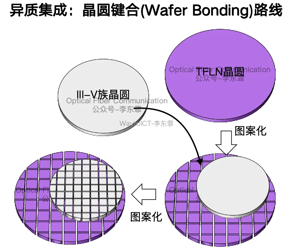
But III-V, lithium niobate, and silicon dioxide have different coefficients of thermal expansion, so the bonding interface is prone to fracture or misalignment at high temperature. BCB can be used as an adhesive layer to reduce process difficulty, with less stringent requirements on surface roughness and cleanliness; however, BCB has poor thermal conductivity and is unfavorable for heat dissipation, and a thicker BCB layer also affects evanescent coupling efficiency.
Compared with hybrid integration, heterogeneous integration uses a vertically stacked structure and typically does not involve flip-chip bumps. But micro-transfer printing, as a transfer process, can also be applied to heterogeneous integration if used to transfer unpatterned III-V thin films. Precisely because heterogeneous integration bonds first and fabricates the laser afterward, it cannot be individually tested before bonding, so its yield still needs improvement.
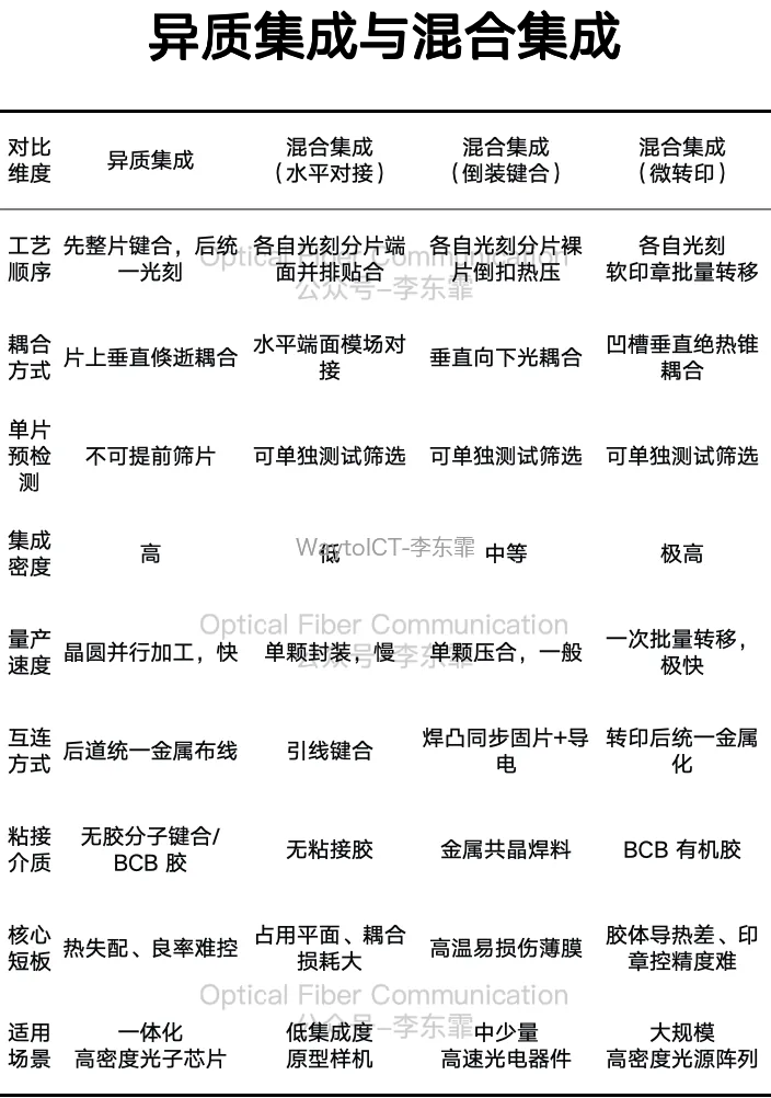
A brief summary comparison of these approaches:
If anything is inaccurate, please point it out. You can add WeChat WaytoICT to join the Semiconductor & Optical Device Industry Group 2.
If you are interested in semiconductors, optical devices, optical modules, and fiber-optic communications, welcome to follow us!
Related Reading
- Basics: How is TFLN thin-film lithium niobate manufactured?
- Hisense: 400Gbps TFLN modulator supporting 3.2T optical modules
- TFLN basics & Huawei HiSilicon’s 540Gbps SiN-SOI-TFLN
Enjoy this article?
Subscribe to get new optical communication insights delivered to your inbox. Free, unsubscribe anytime.