TSMC has proposed a three-dimensional glass waveguide approach for high-density co-packaged optics (CPO) interconnect. The core idea is to use multi-layer waveguide channels inside a glass substrate to solve the mismatch between the optical ports of the optical engine and the fiber ports.
In a CPO package, multiple optical engines surround the ASIC, with fiber array units plugged in at the periphery. The optical ports of the engine and the fiber cores each follow their own arrangement rules, and the two are not necessarily aligned.
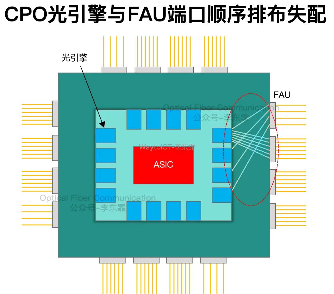
Conventional planar waveguides are usually designed as straight through-routes, so the order of the outer fiber ports must correspond one-to-one with the order of the inner optical engine ports, making rearrangement difficult. When the port sequences do not match, existing approaches either add an external fiber shuffle box, which increases size, loss, and cost, or redesign the chip layout so that it is constrained by the optical port positions, reducing architectural freedom.
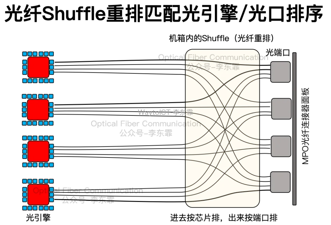
Another problem is crosstalk. In a conventional 2D planar waveguide, all channels lie in the same plane, so crossings are prone to optical coupling and crosstalk, causing signals to interfere with each other.
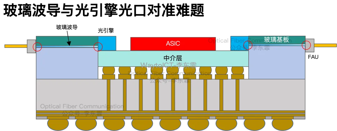
There is also a tolerance problem. Both the glass waveguide and the optical engine chip have thickness fabrication tolerances, and assembly introduces placement offsets. Ideally the inner end face of the glass waveguide aligns directly with the optical engine coupling port, but in practice this is hard to achieve.
To address this, TSMC’s approach leverages the 3D structure: through tilted channels, different inner-end and outer-end heights, and two channels at different heights, the waveguide inner end matches the optical engine port in height, thereby absorbing thickness tolerances and assembly offsets.
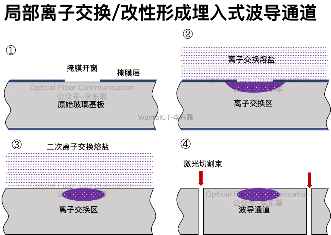
For waveguide formation, TSMC described two approaches. One is the ion-exchange method: in principle, a first mask with a longer time or higher temperature forms a deeper waveguide; after removing the mask, a second mask with a shorter time or lower temperature forms a shallower waveguide.
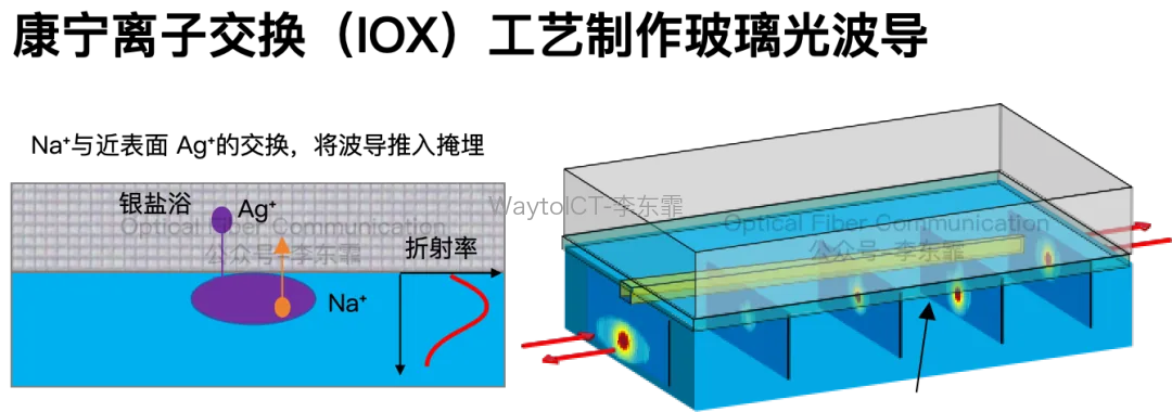
But the ion-exchange method has a drawback: the second thermal treatment or exchange reheats the first waveguide, causing it to diffuse further and widen, so its depth and refractive-index profile change, making control less clean. A similar approach was also described by Corning in its progress on flip-chip CPO packaging for silicon photonic PIC glass substrates.
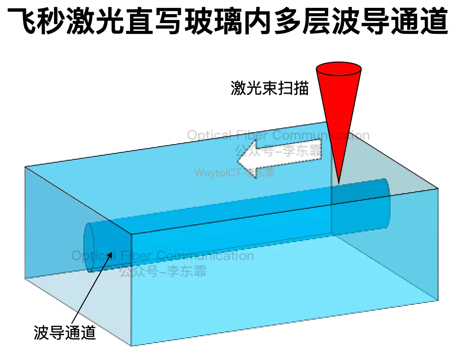
The other route is laser direct writing. Femtosecond laser direct writing writes refractive-index-modified channels at different depths inside the glass by adjusting the focal depth.
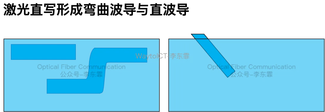
Compared with ion exchange, laser direct writing makes it easier to create curved, straight, and tilted channels in the plane. Curved channels provide in-plane routing freedom, while tilted channels provide height adjustment. Together they mitigate the port height mismatch caused by thickness tolerance and placement offset.
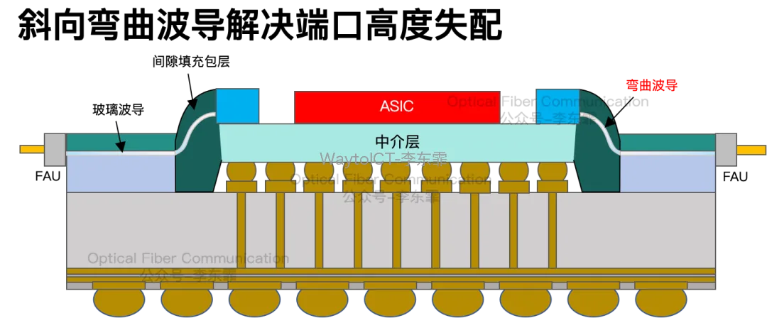
At the coupling interface between the waveguide and the optical engine, an optically transparent adhesive fills the gap between the glass waveguide and the optical engine end face. This reduces Fresnel reflection caused by air gaps and serves as index matching to improve coupling efficiency.
Overall, TSMC’s 3D glass waveguide essentially moves the two long-standing CPO fan-out challenges — port reordering and height alignment — from the chip-layout and external shuffle-box level down into 3D waveguide routing inside the glass substrate. Combined with ion-exchange or femtosecond laser direct writing, it offers a freer and more compact optical interconnect path for high-density, multi-channel CPO scenarios.
Further Reading
- Low-bend-loss glass waveguide process and improvements for CPO
- TSMC: silicon photonic device performance and process platform for CPO
Thanks for reading, and apologies for any inaccuracies.
Enjoy this article?
Subscribe to get new optical communication insights delivered to your inbox. Free, unsubscribe anytime.